
- 25
- Mar
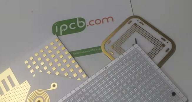
Alumina Ceramic PCB
What are the specific applications of alumina ceramic substrate
In PCB proofing, alumina ceramic substrate has been widely used in many industries. However, in specific applications, the thickness and specification of each alumina ceramic substrate are different. What is the reason for this?
1. The thickness of alumina ceramic substrate is determined according to the function of the product
The thicker the thickness of alumina ceramic substrate, the better the strength and the stronger the pressure resistance, but the thermal conductivity is worse than that of thin one; On the contrary, the thinner the alumina ceramic substrate, the strength and pressure resistance are not as strong as thick ones, but the thermal conductivity is stronger than thick ones. The thickness of alumina ceramic substrate is generally 0.254mm, 0.385mm and 1.0mm/2.0mm/3.0mm/4.0 Mm, etc.
2. The specifications and sizes of alumina ceramic substrates are also different
Generally, alumina ceramic substrate is much smaller than ordinary PCB board as a whole, and its size is generally no more than 120mmx120mm. Those exceeding this size generally need to be customized. In addition, the size of alumina ceramic substrate is not the bigger the better, mainly because its substrate is made of ceramics. In the process of PCB proofing, it is easy to lead to plate fragmentation, resulting in a lot of waste.
3. The shape of alumina ceramic substrate is different
Alumina ceramic substrates are mostly single and double-sided plates, with rectangular, square and circular shapes. In PCB proofing, according to the process requirements, some also need to make grooves on the ceramic substrate and dam enclosing process.
The characteristics of alumina ceramic substrate include:
1. Strong stress and stable shape; High strength, high thermal conductivity and high insulation; Strong adhesion and anti-corrosion.
2. Good thermal cycle performance, with 50000 cycles and high reliability.
3. Like PCB board (or IMS substrate), it can etch the structure of various graphics; No pollution and pollution.
4. Operating temperature range: – 55 ℃ ~ 850 ℃; The coefficient of thermal expansion is close to silicon, which simplifies the production process of power module.
What are the advantages of alumina ceramic substrate?
A. The thermal expansion coefficient of ceramic substrate is close to that of silicon chip, which can save transition layer Mo chip, save labor, materials and reduce cost;
B. Welding layer, reduce thermal resistance, reduce cavity and improve yield;
C. The line width of 0.3mm thick copper foil is only 10% of that of ordinary printed circuit board;
D. The thermal conductivity of the chip makes the package of the chip very compact, which greatly improves the power density and improves the reliability of the system and device;
E. Type (0.25mm) ceramic substrate can replace BeO without environmental toxicity;
F. Large, 100A current continuously passes through 1mm wide and 0.3mm thick copper body, and the temperature rise is about 17 ℃; 100A current continuously passes through 2mm wide and 0.3mm thick copper body, and the temperature rise is only about 5 ℃;
G. Low, 10 × The thermal resistance of 10mm ceramic substrate, 0.63mm thick ceramic substrate, 0.31k/w, 0.38mm thick ceramic substrate and 0.14k/w respectively;
H. High pressure resistance, ensuring personal safety and equipment protection ability;
1. Realize new packaging and assembly methods, so that the products are highly integrated and the volume is reduced.