
- 12
- May
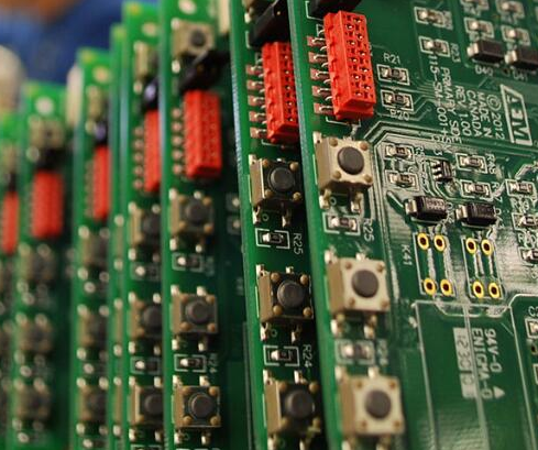
Requirements for PCBA welding processing
PCBA welding processing usually has many requirements for PCB board, which must meet the welding requirements. So why does the welding process require so many requirements for circuit boards? Facts have proved that there will be many special processes in the process of PCBA welding, and the application of special processes will bring requirements to PCB.
If the PCB board has problems, it will increase the difficulty of PCBA welding process, and may eventually lead to welding defects, unqualified boards, etc. Therefore, in order to ensure the smooth completion of special processes and facilitate PCBA welding processing, PCB board must meet the manufacturability requirements in terms of size and pad distance.
Next, I will introduce the requirements of PCBA welding processing on PCB board.
Requirements of PCBA welding processing on PCB board
1. ukuran PCB
The width of PCB (including the edge of circuit board) must be greater than 50mm and less than 460mm, and the length of PCB (including the edge of circuit board) must be greater than 50mm. If the size is too small, it needs to be made into panels.
2. PCB edge width
Plate edge width > 5mm, plate spacing < 8mm, distance between base plate and plate edge > 5mm.
3. PCB bending
Upward bending: < 1.2mm, downward bending: < 0.5mm, PCB deformation: maximum deformation height ÷ diagonal length < 0.25.
4. PCB mark point
Mark shape: standard circle, square and triangle;
Mark size: 0.8 ~ 1.5mm;
Mark materials: gold plating, tin plating, copper and platinum;
Mark’s surface requirements: the surface is flat, smooth, free of oxidation and dirt;
Requirements around mark: there shall be no obstacles such as green oil that is obviously different from the color of the sign within 1mm around;
Mark position: more than 3mm from the edge of the plate, and there shall be no through hole, test point and other marks within 5mm.
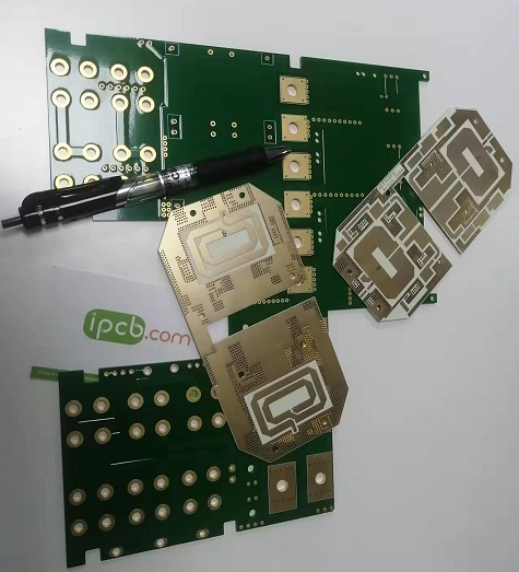
5. PCB pad
There are no through holes on the pads of SMD components. If there is a through hole, the solder paste will flow into the hole, resulting in the reduction of tin in the device, or the tin flows to the other side, resulting in uneven board surface and unable to print the solder paste.
In PCB design and production, it is necessary to understand some PCB welding process knowledge in order to make the products suitable for production. First of all, understanding the requirements of the processing plant can make the subsequent manufacturing process more smooth and avoid unnecessary trouble.
The above is an introduction to the requirements of PCBA welding processing on PCB boards. I hope it can help you and want to know more about PCBA welding processing information.