
- 27
- Apr
What should we pay attention to in PCBA processing? Points needing attention in PCBA processing
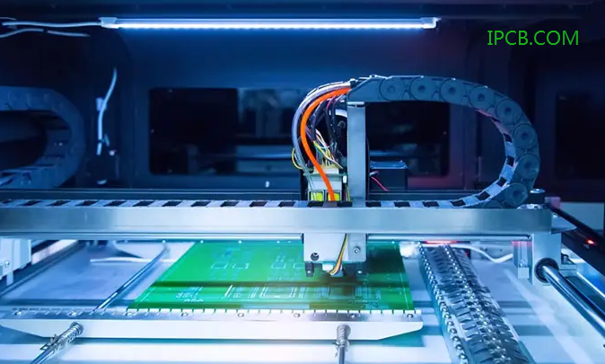
SMT proofing is a professional PCBA processing manufacturer with its own PCB Factory and SMT patch processing factory, which can provide one-stop PCBA processing services such as PCB proofing, component purchasing, SMT patch, dip plug-in, PCBA testing, finished product assembly and so on. Here are the matters needing attention in PCBA processing.
Problems to be considered in PCBA manufacturing
1. Design of single board transmission and positioning elements in automatic production line
For automatic production line assembly, PCBA must have the ability to transmit edge and optical positioning symbols, which is a prerequisite for producibility.
2. PCBA assembly process design
The layout structure of components on the front and back of PCBA determines the process method and path during assembly.
3. Component layout design
Design the position, direction and spacing of components on the assembly surface. The layout of components depends on the welding method adopted. Each welding method has specific requirements for the layout position, direction and spacing of components.
4. Assembly process design
For the design of welding pass through rate, through the matching design of pad, resistance welding and steel mesh, the quantitative and fixed-point stable distribution of solder paste is realized; Through the design of layout and wiring, the synchronous melting and solidification of all solder joints in a single package can be realized; Through the reasonable connection design of the mounting hole, 75% tin penetration rate can be achieved. These design goals are ultimately to improve the welding yield.
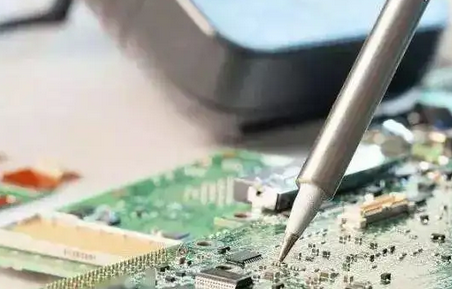
Precautions for PCBA welding
1. The warehouse keeper shall wear anti-static gloves when issuing materials and testing IQC, and the instrument shall be reliably grounded, and the worktable shall be paved with anti-static rubber pad in advance.
2. In the process of operation, anti-static worktops are used, and anti-static containers are used to hold components and semi-finished products. The welding equipment of the Department can be grounded, and the electric soldering iron needs to be of anti-static type. All equipment must be tested before use.
3. When PCBA is processed through the furnace, because the pins of plug-in elements are washed by tin flow, some plug-in elements will tilt after welding, resulting in the element body exceeding the silk screen frame. Therefore, the repair welding personnel after the tin furnace are required to correct it properly.
4. When PCBA is welding horn and battery, it shall be noted that the solder joint shall not be too much, which shall not cause short circuit or falling off of surrounding components.
5. PCBA substrates shall be placed neatly, and bare plates cannot be stacked directly. If stacking is required, it shall be packed in electrostatic bags.
Precautions for PCBA finished product assembly
1. The whole machine without shell uses anti-static packaging bag
Regularly inspect anti-static tools, settings and materials to ensure that the working state meets the requirements.
2. When assembling finished products, follow the following procedures
Warehouse → production line → production line upgrade software → assembly into a complete machine → QC test → write IMEI number → QA full inspection → restore factory settings → warehousing; The software shall be upgraded before assembly. It cannot be assembled into a finished machine and then upgraded. It may not be upgraded due to improper welding, short circuit, operation process problems, etc., resulting in misjudgment of bad PCBA.
The above is what needs attention in PCBA processing? PCBA processing needs to pay attention to the introduction of points, I hope it can help you.