
- 12
- May
PCBA ширетүүчү иштетүү үчүн талаптар
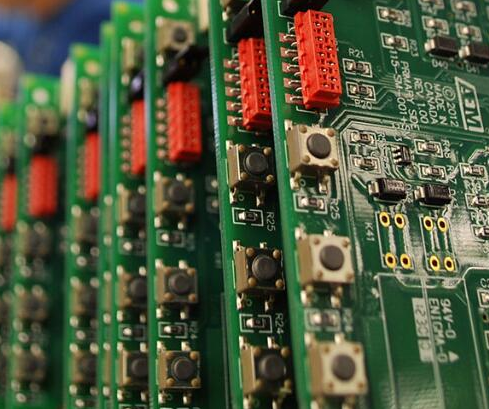
PCBA welding processing usually has many requirements for PCB board, which must meet the welding requirements. So why does the welding process require so many requirements for circuit boards? Facts have proved that there will be many special processes in the process of PCBA welding, and the application of special processes will bring requirements to PCB.
PCB тактасында көйгөйлөр болсо, анда ал PCBA ширетүү процессинин кыйынчылыгын жогорулатат жана акыры ширетүүчү кемчиликтерге, квалификациясыз такталарга ж.б. алып келиши мүмкүн. өлчөмү жана аянтчанын аралыктары боюнча өндүрүштүк талаптарга жооп бериши керек.
Next, I will introduce the requirements of PCBA welding processing on PCB board.
Requirements of PCBA welding processing on PCB board
1. PCB size
The width of PCB (including the edge of circuit board) must be greater than 50mm and less than 460mm, and the length of PCB (including the edge of circuit board) must be greater than 50mm. If the size is too small, it needs to be made into panels.
2. PCB edge width
Пластинанын четинин туурасы > 5 мм, плиталардын аралыгы < 8 мм, базалык плита менен плитанын четинин ортосундагы аралык > 5 мм.
3. PCB bending
Upward bending: < 1.2mm, downward bending: < 0.5mm, PCB deformation: maximum deformation height ÷ diagonal length < 0.25.
4. PCB белги чекити
Mark shape: standard circle, square and triangle;
Белги өлчөмү: 0.8 ~ 1.5 мм;
Mark materials: gold plating, tin plating, copper and platinum;
Mark’s surface requirements: the surface is flat, smooth, free of oxidation and dirt;
Белгинин айланасындагы талаптар: айланасында 1 мм чегинде белгинин түсүнөн ачык айырмаланган жашыл май сыяктуу эч кандай тоскоолдуктар болбошу керек;
Марктын абалы: пластинанын четинен 3мм ашык жана 5мм ичинде тешик, сыноо чекити жана башка белгилер болбошу керек.
5. PCB pad
There are no through holes on the pads of SMD components. If there is a through hole, the solder paste will flow into the hole, resulting in the reduction of tin in the device, or the tin flows to the other side, resulting in uneven board surface and unable to print the solder paste.
ПХБ дизайнында жана өндүрүшүндө, өнүмдөрдү өндүрүшкө ылайыктуу кылуу үчүн кээ бир PCB ширетүү процессин билүү керек. Биринчиден, кайра иштетүүчү ишкананын талаптарын түшүнүү кийинки өндүрүш процессин жылмакай кылып, ашыкча кыйынчылыктардан качууга жардам берет.
The above is an introduction to the requirements of PCBA welding processing on PCB boards. I hope it can help you and want to know more about PCBA welding processing information.