- 23
- Mar
HDI (High Density Interconnect) PCB board
What is an HDI (High Density Interconnect) PCB board?
High density Interconnect (HDI) PCB, is a kind of printed circuit board production (technology), the use of micro-blind hole, buried hole technology, a circuit board with relatively high distribution density. Due to the continuous development of technology for high-speed signal electrical requirements, the circuit board must provide impedance control with ac characteristics, high frequency transmission capability, reduce unnecessary radiation (EMI) and so on. Using Stripline, Microstrip structure, multi-layer design becomes necessary. In order to reduce the quality problem of signal transmission, the insulation material with low dielectric coefficient and low attenuation rate will be adopted. In order to match the miniaturization and array of electronic components, the density of the circuit board will be increased continuously to meet the demand.
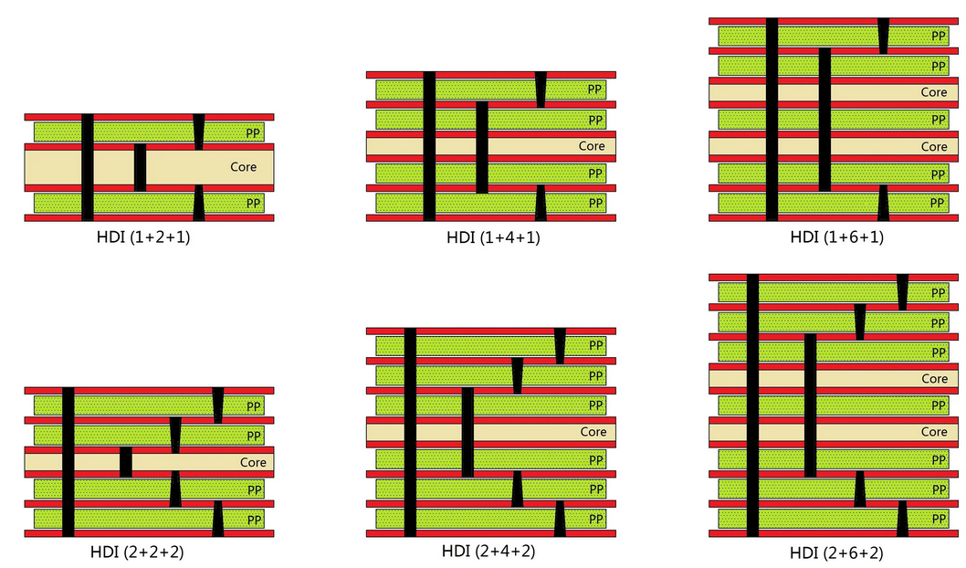
HDI (high density interconnection) circuit board usually includes laser blind hole and mechanical blind hole;
Generally through buried hole, blind hole, overlapping hole, staggered hole, cross buried hole, through hole, blind hole filling electroplating, thin line small gap, plate microhole and other processes to achieve the conduction between the inner and outer layers, usually the blind buried diameter is not greater than 6mil.
HDI circuit board is divided into several and any layer interconnection
First-order HDI structure: 1+N+1 (pressing twice, laser once)
Second-order HDI structure: 2+N+2 (pressing for 3 times, laser for 2 times)
Third order HDI structure: 3+N+3 (pressing 4 times, laser 3 times)Fourth order
HDI structure: 4+N+4 (pressing 5 times, laser 4 times)
And anylayer HDI