
- 19
- May
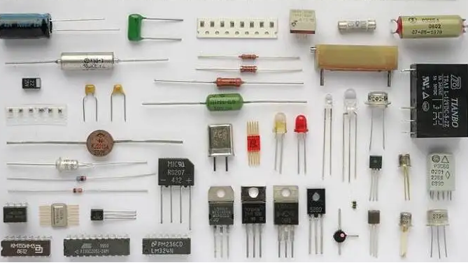
On line pin sequence of electronic components
For the vast majority of electronic components, they have polarity, or the pins can not be soldered wrong. For example, once the electrolytic capacitor is welded reversely, it will explode when energized. Generally speaking, when using automatic feeding machinery to assemble circuit board components, there will be no problem of misplacing components. However, due to the limitations of manufacturers and the characteristics of components, not all components can be automatically pasted or inserted. Common manual placement is required for various surface mounted transformers, connectors, to encapsulated integrated circuits, etc. These devices may still have the problem of assembly error. Generally, the repair is carried out manually, and this link is also prone to the problem of reverse welding. Therefore, it is necessary to explain the positioning method of components and the corresponding relationship between component pads and silk screen printing on the circuit board.
1. اہلیت
For the electrolytic capacitor installed in the aluminum through hole shown in the figure below, the positive and negative poles are generally represented by the long and short feet and the mark on the body. The long leg is positive and the short leg is negative. Generally, there are white or other stripes parallel to the pin on the shell of the negative side.
سرکٹ بورڈ پر الیکٹرولائٹک کیپسیٹر کو عام طور پر پولرٹی کے ساتھ نشان زد کیا جاتا ہے جیسا کہ تصویر میں دکھایا گیا ہے۔
ایک طریقہ یہ ہے کہ “+” نشان کو براہ راست مثبت پہلو پر نشان زد کریں۔ اس طریقہ کار کا فائدہ یہ ہے کہ ویلڈنگ کے بعد قطبیت کی جانچ کرنا آسان ہے۔ نقصان یہ ہے کہ یہ سرکٹ بورڈ کے ایک بڑے حصے پر قابض ہے۔ دوسرا طریقہ اس علاقے کو بھرنا ہے جہاں منفی الیکٹروڈ سلک اسکرین کے ساتھ واقع ہے۔ پولرٹی کی یہ نمائندگی سرکٹ بورڈ کے ایک چھوٹے سے علاقے پر قابض ہے، لیکن ویلڈنگ کے بعد قطبیت کی جانچ کرنا تکلیف دہ ہے۔ یہ سرکٹ بورڈ ڈیوائسز جیسے کمپیوٹر مدر بورڈ کی زیادہ کثافت والے مواقع میں عام ہے۔
Tantalum capacitors installed through holes are generally marked with “+” on the body on the positive side, and some varieties are further distinguished by long and short feet.
اس کیپسیٹر کے سرکٹ بورڈ پر مارکنگ کا طریقہ ایلومینیم الیکٹرولائٹک کپیسیٹر کا حوالہ دے سکتا ہے۔
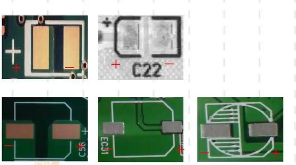
For surface mounted aluminum electrolytic capacitors. The side coated with ink is the negative pole, and the base on the positive pole side is generally chamfered.
 پر پرنٹ سرکٹ بورڈ، یہ عام طور پر اوپر کی شکل میں دکھایا گیا ہے۔
That is to use silk screen “+” on the circuit board to represent the positive pole, and draw the outline of the device at the same time. In this way, the chamfered side can also be used to identify the positive electrode.
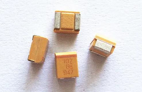
سطح سے منسلک ٹینٹلم کیپسیٹر
2. ڈائیوڈ
روشنی خارج کرنے والے ڈائیوڈس کے لیے، لمبے اور چھوٹے پن کو عام طور پر مثبت اور منفی قطبوں کی نمائندگی کرنے کے لیے استعمال کیا جاتا ہے۔ لمبا پن مثبت ہے اور چھوٹا پن منفی ہے۔ بعض اوقات کارخانہ دار ایل ای ڈی کے ایک طرف سے تھوڑا سا کاٹ دیتا ہے، جسے منفی الیکٹروڈ کی نمائندگی کرنے کے لیے بھی استعمال کیا جا سکتا ہے۔
سلک اسکرین “+” عام طور پر سرکٹ بورڈ پر مثبت الیکٹروڈ کی نشاندہی کرنے کے لیے استعمال ہوتی ہے۔
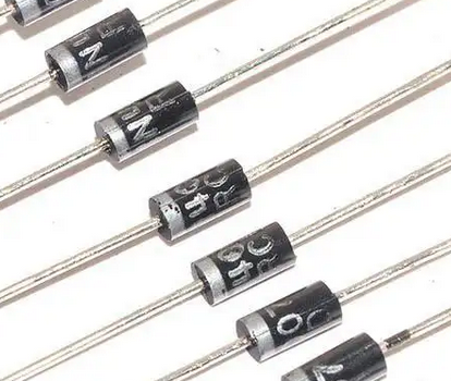
عام ڈایڈس کے لیے
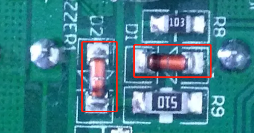
In the figure above, the left side is the negative pole and the right side is the positive pole, that is, silk screen printing or stained glass is used to represent the positive and negative polarity. The following two methods are generally used to represent the positive and negative polarity on the circuit board.
The polarity of the diode is indicated by the silk screen on the circuit board. This is more vivid. The other is to draw the schematic symbols of diodes directly on the silk screen چھپی سرکٹ بورڈ.
سطح پر نصب ایل ای ڈی کی قطبیت کی نمائندگی بہت مبہم ہے۔ بعض اوقات کارخانہ دار میں مختلف پیکیج کی اقسام کے درمیان مختلف نمائندگی ہوتی ہے۔ تاہم، روشنی خارج کرنے والے ڈائیوڈس کے کیتھوڈ سائیڈ پر رنگین دھبوں یا رنگ کی پٹیوں کو پینٹ کرنا عام بات ہے۔ کیتھوڈ سائیڈ پر بھی کونے کٹے ہوئے ہیں۔
The polarity of the diode is indicated by the silk screen on the circuit board. This is more vivid. The other is to draw the schematic symbols of diodes directly on the silk screen printed circuit board.
سطح پر نصب ایل ای ڈی کی قطبیت کی نمائندگی بہت مبہم ہے۔ بعض اوقات کارخانہ دار میں مختلف پیکیج کی اقسام کے درمیان مختلف نمائندگی ہوتی ہے۔ تاہم، روشنی خارج کرنے والے ڈائیوڈس کے کیتھوڈ سائیڈ پر رنگین دھبوں یا رنگ کی پٹیوں کو پینٹ کرنا عام بات ہے۔ کیتھوڈ سائیڈ پر بھی کونے کٹے ہوئے ہیں۔
Ordinary surface mount diodes also use silk screen printing or stained glass on the body to represent the negative electrode
مربوط سرکٹ
ڈِپ اور اسی طرح پیکڈ انٹیگریٹڈ سرکٹس کے لیے جس میں پن دونوں طرف تقسیم کیے گئے ہیں، بالائی سیمی سرکلر نوچ کا استعمال عام طور پر یہ بتانے کے لیے کیا جاتا ہے کہ یہ سمت چپ کے اوپر ہے، اور اوپری بائیں جانب پہلا پن چپ کا پہلا پن ہے۔ یہ سلک اسکرین پرنٹنگ یا لیزر کے ساتھ سب سے اوپر ایک افقی لکیر سے بھی ظاہر ہوتا ہے۔
In addition, there are also silk screen dots directly on the body next to the first pin of the chip or pressing a pit directly during injection molding.
کچھ انٹیگریٹڈ سرکٹس کو پہلے پن کے ابتدائی کنارے کے باڈی پر بیولڈ کنارے کاٹ کر بھی دکھایا جاتا ہے۔
The symbols of this kind of integrated circuit on the circuit board are generally marked with a gap on the top.
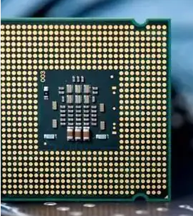
For QFP, PLCC and BGA in tetragonal package.
QFP پیکڈ انٹیگریٹڈ سرکٹس عام طور پر ماڈل کے مطابق مقعر نقطوں، سلک اسکرین ڈاٹس، یا سلک اسکرین پرنٹنگ کا استعمال کرتے ہیں تاکہ جسم کی سمت پہلے پن کے مطابق ہو۔ کچھ پہلے پاؤں کی نمائندگی کرنے کے لیے زاویہ کو کاٹنے کا طریقہ استعمال کرتے ہیں۔ اس وقت، گھڑی کی مخالف سمت پہلا پاؤں ہے۔ واضح رہے کہ بعض اوقات ایک چپ پر تین گڑھے ہوتے ہیں، اس لیے گڑھے کے بغیر ایک کونا چپ کے نچلے دائیں سے مساوی ہوتا ہے۔
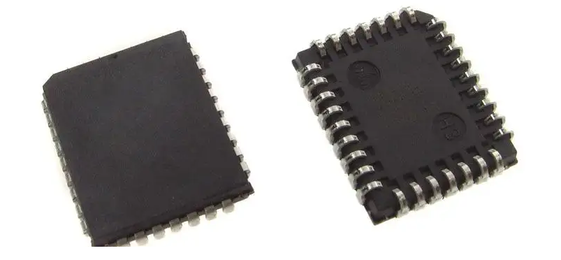
Because the body of PLCC package is relatively large, it is generally represented by pits directly at the beginning of the first pin. Some also cut corners at the top left of the chip.
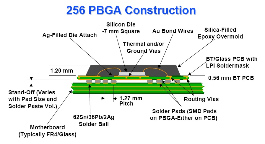
BGA پیکڈ آبجیکٹ
BGA packaging not only uses the gold-plated copper foil in the lower left corner to represent the first pin, but also uses the way of missing corners, pits and silk screen dots to represent the direction of the first pin.
متعلقہ سرکٹ بورڈ پر گرافکس درج ذیل ہیں۔
 پہلی ٹانگ کا علاج سلک اسکرین کے نقطوں اور گمشدہ کونوں سے کیا جاتا ہے۔
4. دیگر آلات
اصلی آبجیکٹ میں، کنیکٹر عام طور پر نشان کو پوزیشن میں رکھ کر سمت کو کنٹرول کرتا ہے۔ ایسے بھی ہیں جو پہلے پاؤں کے قریب 1 لکھتے ہیں یا پہلے پاؤں کی نمائندگی کے لیے مثلث استعمال کرتے ہیں۔ عام طور پر، دوسرے آلات ریشم کی سکرین کو اصلی آبجیکٹ کے مطابق بنا کر غلط اندراج سے بچتے ہیں۔ چھپی سرکٹ بورڈ.
For the resistance removal of through-hole installation, it is generally expressed by wrapping the common end with silk screen on the circuit board. Or write 1 near the first foot.
سرکٹ بورڈ پر پیڈ، سلک اسکرین پرنٹنگ اور اجزاء کی مزاحمتی ویلڈنگ کی ضروریات کو معیاری بنانے کے لیے، IPC تنظیم نے دو متعلقہ معیارات جاری کیے ہیں: ipc-7351 اور ipc-sm-840۔ تاہم، اصل استعمال میں، آئی پی سی کے ذریعہ بیان کردہ ڈیوائس کی سمت کی نمائندگی کے طریقہ کار کے ذریعہ بنائے گئے آلے کی سمت مارکنگ علامتیں اکثر ویلڈنگ کے بعد ڈیوائس باڈی کے ذریعہ بلاک کردی جاتی ہیں، جو معائنہ کے لیے موزوں نہیں ہیں۔ اجزاء پیڈ کے گرافک ڈیزائن کو اصل صورت حال کے مطابق ایڈجسٹ کیا جانا چاہئے.
In short, in real objects, generally discrete devices use the methods of long and short feet, silk screen printing or coloring to represent the polarity. For integrated circuits, concave points, silk screen printing, notches, missing corners, missing edges or direct indication are often used for the first pin marking. When making pad graphics, generally draw according to the device shape as much as possible, and reflect the information related to positioning on the device shape in the form of silk screen as much as possible, so as to avoid errors in manual assembly and welding.