
- 23
- Oct
PCB Design–Right-Angle Alignment
Right-angle alignment is generally required in PCB wiring to avoid the situation, but also almost become one of the standards to measure of good or bad wiring, then the right-angle signal transmission will actually have much impact on it?
The impact of right-angle alignment on the signal is mainly reflected in three aspects:
I. It can be equated to a capacitive load on the transmission line, slowing down the rise time;
II.The impedance discontinuity will cause signal reflection;
III. The EMI generated by right-angle tip.
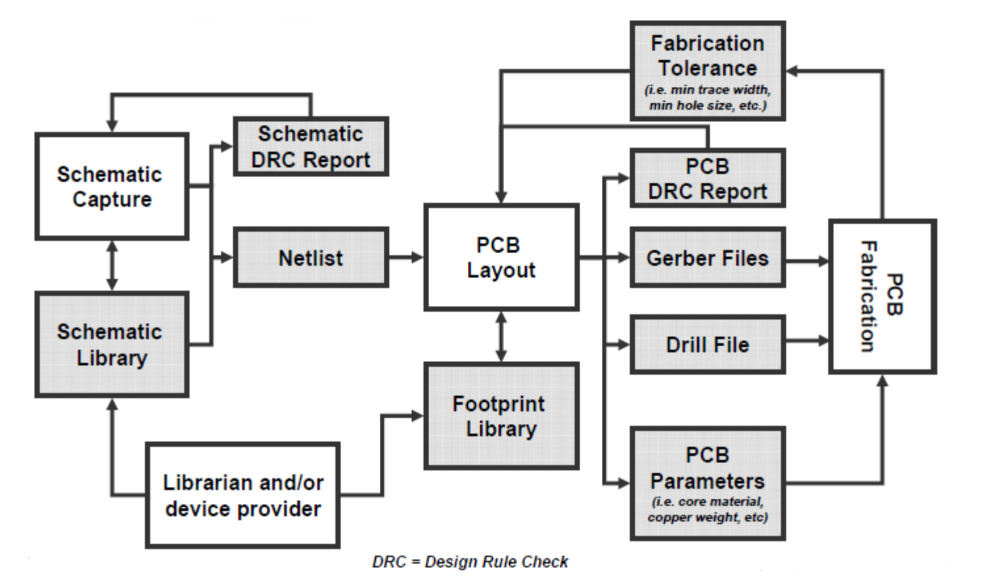
The PCB Design Flow
The parasitic capacitance due to the right angle of the transmission line can be calculated by the following empirical formula:
C=61W(Er)[size=1]1/2[/size]/Z0
C the equivalent capacitance of the corner (unit: pF):W refers to the width of the alignment (unit: inch):εr refers to the dielectric constant of the medium:Z0 the characteristic impedance of the transmission line.
The calculations show that the capacitive effect from a right-angle alignment is extremely small. However, right-angle alignments are not as scary as one might think. At least in sub-GHz applications, any effects such as capacitance, reflections, EMI, etc., are barely noticeable in TDR tests, and the focus of the high-speed PCB design engineer is still on the straight line.
High-Speed PCB design engineers should still focus on layout, power/ground design, alignment design, vias, and other aspects. Of course, although the impact of right-angle alignment is not very serious, but does not mean that we can go straight line, attention to detail is the basic quality of each good engineer must have. With the rapid development of digital circuits, PCB engineers to deal with the frequency of the signal will continue to improve, to more than 10GHz RF design areas, these small right angles may become the focus of high-speed issues.
All in all, iPCB provides one-stop service from PCB design to PCBA assembly, please contact us if you need.