
- 07
- Apr
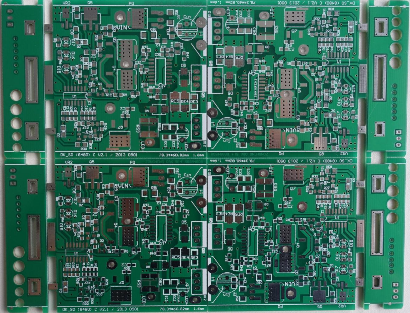
Mastering Current Loops in PCB Design
Introduction: PCB (Printed Circuit Board) design requires meticulous attention to detail, especially when it comes to managing current loops. A thorough understanding of current flow and its implications is crucial for ensuring optimal performance and reliability of electronic systems. In this blog post, we will delve into the key precautions and strategies for managing current loops effectively in PCB designs, demystifying complex concepts and offering practical insights for engineers.
- Optimal Wiring Thickness: When considering wiring for ground connections on the PCB, it’s essential to prioritize thickness. Thicker wiring minimizes resistance and inductance, facilitating efficient current flow. Remember that the minimum width of the ground wire should be calculated from the farthest point to the power connection.
- Avoiding Ground Loops: Ground loops can introduce unwanted noise and interference, compromising the integrity of signals. To mitigate this risk, ensure that your PCB layout avoids creating loops in the ground path. Implementing a star connection strategy, where each component has an independent path to the power connection, is recommended.
- Star Connection Strategy: In situations where utilizing a ground plane isn’t feasible, adopting a star connection strategy becomes paramount. This approach ensures that ground currents return to the power connection independently, minimizing the risk of interference between components. Refer to Figure 6 for a visual representation of this strategy.
- Digital-Analog Segregation: Separating digital and analog devices is crucial for maintaining signal integrity. Digital circuits often generate high-frequency currents, leading to voltage fluctuations in the ground plane. These fluctuations can adversely affect analog signals. By keeping digital and analog currents separate, you prevent interference and preserve signal quality.
- High-Speed vs. Low-Speed Devices: Distinguishing between high-speed and low-speed devices is essential when routing current paths. High-speed circuits introduce rapid current changes, resulting in voltage fluctuations along the ground plane. When these fluctuations propagate through low-speed devices, they can distort signals. To mitigate this, ensure that high-speed and low-speed circuits have separate ground paths.
Practical Considerations:
- Utilize ground planes whenever possible to provide a low-impedance return path for currents.
- Employ proper decoupling capacitors near integrated circuits to suppress voltage fluctuations.
- Pay attention to signal integrity by minimizing signal loop area and avoiding crossing high-speed and low-speed signal traces.
Conclusion: Mastering current loops in PCB design is a fundamental skill for engineers seeking to optimize electronic systems’ performance and reliability. By adhering to the precautions and strategies outlined in this blog post, you can effectively manage current flow, minimize interference, and ensure signal integrity in your PCB designs. Remember, meticulous attention to detail during the design phase pays dividends in the form of robust and efficient electronic systems.