
- 20
- Sep
Key points of PCB compatibility design
Key points of PCB compatibility design:
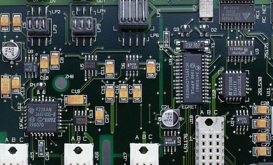
1, circuit board compatibility is mainly reflected in electromagnetic compatibility, and electromagnetic compatibility can be understood as the circuit board in a variety of electromagnetic environment can maintain the ability to coordinate and work effectively, first of all, the first influence circuit board electromagnetic compatibility is wire width, wire width determines the inductance composition of printed wire, Inductance composition determines the impact interference capacity of transient current on the circuit board, so a reasonable choice of wire width can minimize the electromagnetic interference.
2, in addition to the inductance, printed wiring can influence on the circuit board wiring is also affects inductance, such as the more common is equal walk the line, so that we can have the effect of reducing inductance, mutual inductance increases, but the downside is wires but also increase the number of capacitance, so in the design of circuit board, should according to the specific situation to choose the most reasonable wiring.
3, besides just mentioned inductance, influence and lead of the papan sirkuit compatibility, the crosstalk between the need to pay attention to this area is still a wiring, such as just mentioned equal wiring will try to avoid long distance equal wiring, and then try to let the distance between line and line, as well as signal wire and ground wire and the power cord do not cross, If there is a very sensitive signal cable, you can add a suppression cable to avoid crosstalk, which can also effectively suppress crosstalk.