
- 26
- Mar
The Advantages and Disadvantages of PCB Copper Cladding
Introduction:
In the realm of PCB (Printed Circuit Board) design, copper cladding plays a pivotal role in ensuring optimal performance and reliability. However, like any design element, it comes with its own set of advantages and disadvantages that designers must carefully consider. Let’s delve into the intricacies of copper cladding to understand how it impacts PCB functionality and performance. 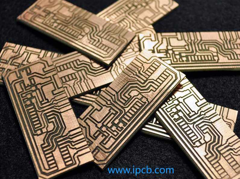
Advantages of Copper Cladding:
- Impedance Reduction and Anti-Interference: Copper cladding serves as a vital component in reducing impedance in ground wires and enhancing the PCB’s anti-interference capabilities. By filling unused spaces with solid copper, designers can effectively lower the impedance of ground connections, thus minimizing signal distortion and ensuring reliable performance even in noisy environments.
- Voltage Drop Reduction: Another significant advantage of copper cladding is its ability to mitigate voltage drop, consequently improving the efficiency of power supplies. By providing a low-resistance pathway for current flow, copper cladding helps maintain stable voltage levels across the PCB, ensuring consistent operation of connected components.
- Enhanced Grounding: Properly implemented copper cladding facilitates robust grounding, which is essential for reducing loop area and minimizing electromagnetic interference (EMI). Grounded copper areas act as shields, preventing unwanted signal coupling and maintaining signal integrity throughout the PCB.
- Soldering Stability: Copper cladding also aids in stabilizing the PCB during soldering processes. By filling open areas with copper, designers ensure uniform heat distribution, minimizing the risk of warping or distortion during assembly.
Disadvantages of Copper Cladding:
- High-Frequency Challenges: In high-frequency circuits, copper cladding can inadvertently exacerbate noise issues if not implemented judiciously. The distributed capacitance of PCB traces can lead to antenna effects, causing noise to propagate through the copper cladding and interfere with circuit operation.
- Grid Copper Limitations: While grid copper offers benefits such as improved heat dissipation and electromagnetic shielding, it may not be suitable for all applications. The staggered traces in grid copper configurations can introduce electrical length mismatches, potentially leading to signal integrity issues and operational failures, especially at higher frequencies.
- Wave Soldering Concerns: Large-area copper cladding, while effective in enhancing current capacity and shielding, may pose challenges during wave soldering processes. The accumulation of heat can cause the PCB to lift or blister, necessitating the addition of relief grooves to mitigate these issues.
Navigating Copper Cladding Choices:
In determining the optimal copper cladding strategy for a PCB design, designers must carefully evaluate the specific requirements and constraints of their application. High-frequency circuits demand meticulous attention to grounding and signal integrity, making grid copper a preferred choice for mitigating interference. Conversely, low-frequency circuits with high current requirements may benefit from extensive large-area copper cladding to facilitate efficient current flow.
Ultimately, the key to harnessing the advantages of copper cladding lies in striking a balance between functionality, manufacturability, and performance. By understanding the nuances of copper cladding and its impact on PCB design, designers can make informed decisions that optimize both the electrical and mechanical characteristics of their designs.
In conclusion, while copper cladding presents both advantages and disadvantages, its judicious application is indispensable for achieving optimal PCB performance and reliability across a diverse range of applications. By leveraging its strengths and mitigating its limitations, designers can craft PCB layouts that deliver robust functionality and meet the stringent demands of modern electronics.