
- 02
- Feb
Navigating the Depths of Multi-Layer PCB Design
Introduction
In the ever-evolving landscape of electronic product development, the importance of a well-designed Printed Circuit Board (PCB) cannot be overstated. As technology advances, so does the demand for compact, intelligent, and high-performance electronic devices. One crucial aspect of meeting these demands is the utilization of multi-layer PCBs, which provide the flexibility, stability, and reliability required for cutting-edge electronics.
Understanding Multi-Layer PCBs
What Sets Multi-Layer PCBs Apart?
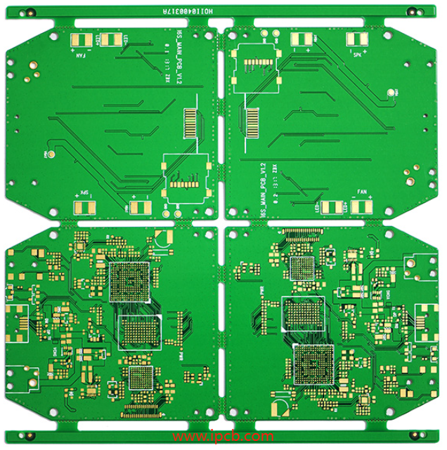
Multi-layer PCBs, as the name suggests, consist of more than two layers of conductive material separated by insulating substrates. These boards offer a myriad of advantages, including enhanced space efficiency, improved signal integrity, and the ability to accommodate advanced Surface Mount Devices (SMD) such as QFP, QFN, CSP, and BGA.
Evolution from SLC to HDI Microplates
The journey of multi-layer PCBs traces back to 1991 when IBM pioneered high-density multilayer technology. Since then, various global entities have contributed to the development of High-Density Interconnect (HDI) microplates. This rapid progress has revolutionized PCB industrial technology, leading to the widespread adoption of multi-layer boards in electronic product manufacturing.
Essential Steps Before Embarking on PCB Design
1. Thoroughly Validate the Schematic Diagram
The foundation of any successful PCB design lies in the accuracy of the schematic diagram. Before delving into the design process, meticulous checks and validations of the schematic are imperative. This ensures the correct interconnection of devices, paving the way for a flawless PCB layout.
2. Prudent Device Selection
The selection of components plays a pivotal role in the success of PCB design. Components with identical functions may differ in packaging methods, influencing the layout of solder holes on the board. Hence, it is crucial to determine the packaging form of each component before initiating the design process.
3. Strategic Positioning of SMDs in Multilayer Boards
In the realm of multi-layer PCBs, the strategic placement of Surface Mount Devices (SMDs) holds paramount importance. SMDs, known for their miniaturization, high integration, reliability, and automated installation, are extensively used in electronic products. During device selection, attention must be paid not only to meeting circuit requirements but also ensuring a stable supply chain to prevent potential component shortages.
4. Embracing Domestic Components
As the quality of domestic electronic components continues to rise, considering them for the PCB design becomes a prudent choice. Items such as chip resistors, capacitors, and connectors have reached levels comparable to their imported counterparts. With advantages like ample supply, short delivery times, and cost-effectiveness, opting for domestic components is a strategic move, provided they meet the circuit’s specifications.
Conclusion
In the dynamic world of electronics, where innovation is relentless, mastering the intricacies of multi-layer PCB design is a necessity. By focusing on schematic accuracy, careful component selection, strategic SMD placement, and embracing domestic components, designers can create PCBs that not only meet the demands of modern electronics but also pave the way for future advancements. The journey from schematic to a functional multi-layer PCB is an art and science that transforms concepts into tangible, high-performance electronic devices.