
- 04
- Feb
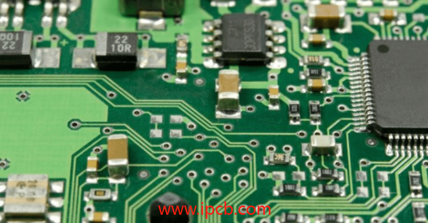
Mastering SMT-PCB Design
Introduction: Welcome to the world of Surface Mount Technology (SMT) and Printed Circuit Board (PCB) design! In this blog, we’ll explore key principles that will help you optimize the layout of components on your SMT-PCB, ensuring a smooth manufacturing process and robust circuit performance.
- Component Layout for Reflow Soldering:
When placing your PCB on the reflow soldering conveyor, align the long axis of components perpendicular to the equipment’s transmission direction. This prevents the notorious “tombstone” effect, where components can drift during soldering.
Ensure an even distribution of components across the PCB, with special attention to dispersing high-power components. This prevents local overheating, safeguarding the reliability of solder joints and overall circuit functionality.
For double-sided components, stagger larger elements on each side to avoid welding issues caused by increased local heat capacity during the process.
Devices with pins on all four sides, such as PLCC/QFP, should not be placed on the wave soldering surface.
Large SMT devices on the wave soldering surface should have their long axis parallel to the solder wave flow direction, reducing solder bridging between electrodes.
Stagger large and small SMT components on the wave soldering surface to prevent false soldering and missing soldering due to the “shadow” effect of the solder wave crest.
- Pad Design for SMT Components:
Enlarge pads for larger components on the wave soldering surface to prevent the “shadow effect” and subsequent empty welds.
Adjust pad size according to component dimensions, ensuring that the pad width is equal to or slightly larger than the electrode width for optimal soldering.
Avoid using a single large pad between interconnected components, as solder on the large pad may connect the components in the middle. Instead, separate the pads and connect them with a thinner wire. For higher current requirements, parallel wires covered with green oil can be used.
Eliminate through holes on or near SMT component pads to prevent solder flow issues during the reflow process, reducing the risk of false soldering, insufficient tin, or short circuits.
Conclusion: By incorporating these SMT-PCB design principles, you’ll pave the way for a seamless manufacturing process and enhance the reliability of your electronic circuits. Whether you’re a seasoned PCB designer or just diving into the world of SMT, these guidelines will empower you to create robust and efficient designs for your electronic projects.