
- 31
- Jan
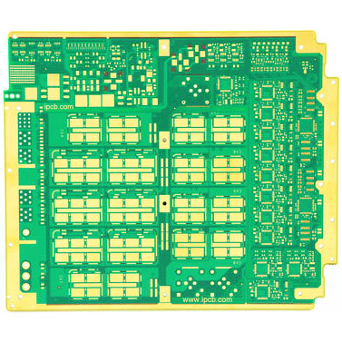
Navigating Signal Integrity Challenges in Flexible PCB Design
Introduction:
In the ever-evolving landscape of electronics, Flexible Printed Circuit Boards (PCBs) have emerged as integral components due to their versatility and space-saving capabilities. As these boards become increasingly prevalent, the need for high-speed signal transmission on flexible substrates has become inevitable. However, this transition comes with its set of challenges, particularly in managing signal integrity. In this blog post, we will delve into the intricacies of signal integrity in PCB design, focusing on the interplay between flexible and rigid-flex PCBs, ground plane strategies, impedance control, and the impact of grid patterns.
Flexible and Rigid-Flex PCBs: A Balancing Act
As the demand for flexible PCBs rises, designers face the challenge of maintaining signal integrity while accommodating the bending and folding nature of these boards. A common approach involves employing shadowed line or grid-like ground planes on flexible ribbons. This technique ensures a consistent 0V reference, shielding over a broad frequency range, and flexibility for bending without compromising rigidity.
However, signal integrity issues may arise, particularly in wiring impedance, shielding, and isolation. This calls for a careful consideration of the grid floor plan design to strike a balance between impedance control and the flexibility required for the application.
Grid Grounding Plane: A Critical Element
The grid grounding plane plays a crucial role in providing a consistent reference for signal traces, whether on flexible or rigid-flex PCBs. The mesh structure of the grid, while not commonly seen in rigid boards, becomes essential in flexible applications to address impedance control and flexibility concerns.
Impedance Control Strategies:
Designers face choices in impedance control strategies, with the option of using a solid copper layer directly below the wiring or incorporating a grid structure elsewhere in the circuit. The geometric parameters of the grid, specifically L (grid opening) and W (grid width), influence impedance and flexibility. Adjusting these parameters allows designers to fine-tune the performance of the flexible ribbon, ensuring optimal impedance while maintaining flexibility.
Fiber Braiding Concerns:
An intriguing aspect arises when the grid grounding plane starts resembling the glass-woven pattern seen in traditional laminates. This raises concerns about fiber braiding effects, particularly when the signal frequency overlaps with resonances in the mesh. The grid structure, similar to glass weaving, can lead to resonance-related issues, creating challenges in maintaining signal integrity.
Resonance and EMI Challenges:
The grid grounding plane introduces resonant cavities that can support high-Q resonance, leading to increased cavity emissions and power losses. Open grid structures may have lower isolation, allowing radiated EMI along the surface of the flexible carbon band. To mitigate these challenges, designers can opt for a tighter mesh, similar to tighter glass braiding, to prevent fiber braiding effects and enhance overall signal integrity.
Conclusion:
As flexible PCBs become increasingly sophisticated with advancements in manufacturing capabilities, understanding and addressing signal integrity challenges are paramount. Designers must carefully navigate the interplay between flexible and rigid-flex PCBs, leverage effective grid grounding plane strategies, and employ impedance control measures to ensure seamless high-speed signal transmission. By doing so, we pave the way for the continued evolution of flexible PCBs in the ever-expanding realm of electronic applications.