
- 16
- Sep
How to distinguish the number of pcb layers
The substrate of the PCB board itself is made of insulating and heat-insulating materials that are not easy to bend. The small circuit material that can be seen on the surface is copper foil. The copper foil was originally covered on the entire PCB board, but part of it was etched away during the manufacturing process, and the remaining part became a network of small circuits NS. These lines are called wires or wiring, and are used to provide circuit connections for parts on the PCB.
Usually the color of PCB board is green or brown, which is the color of solder mask. It is an insulating protective layer that can protect the copper wire and prevent parts from being welded to the wrong place. Multilayer boards are now used on motherboards and graphics cards, greatly increasing the area that can be wired.
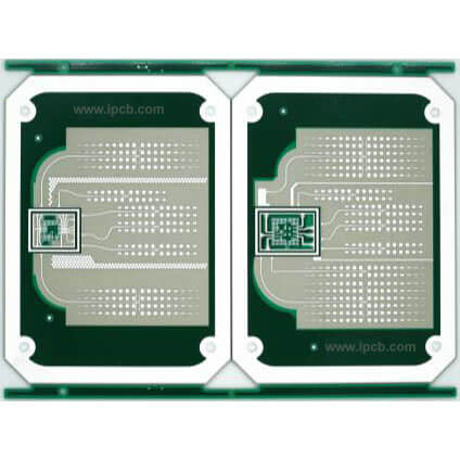
How to distinguish the number of layers of the motherboard PCB board
Steps/Methods
Multilayer boards use more single or double-sided wiring boards, and put a layer of insulating layer between each layer of boards and press them together.
How to distinguish the number of layers of the motherboard PCB board
2
The number of layers of the PCB board means that there are several independent wiring layers. Usually the number of layers is even and contains the two outermost layers. Common PCB boards generally have a structure of 4 to 8 layers. The number of layers of many PCB boards can be seen by looking at the cut surface of the PCB board. But in fact, no one can have such good eyesight. So, let me teach you one more method below.
3
The circuit connection of the multi-layer board is through buried via and blind via technology. Most motherboards and display cards use 4-layer PCB boards, and some use 6, 8-layer, or even 10-layer PCB boards.
4
If you want to see how many layers the PCB has, you can identify it by observing the via holes, because the 4-layer boards used on the motherboard and display card are traces on the first and fourth layers, and the other layers have other uses (ground wires). And power supply). Therefore, like the double-layer board, the via hole will penetrate the PCB bhodhi.
5
If some vias appear on the front of the PCB but cannot be found on the reverse, then it must be a 6/8-layer board. If the same via holes can be found on both sides of the PCB, it will naturally be a 4-layer board.