
- 18
- Sep
PCB-productieproces
1. Selecteer de SCH or PCB file name (in English and digits) and add the extension name.
2. Schematic diagram first design the size of the grid, the size of the drawing, choose metric system, add good library components. Draw diagrams, components, and lines according to the functional modules of the circuit in such a way that it is easy to see the principle. As far as possible uniform, beautiful, do not walk wire inside the component, pay attention to do not walk wire in the middle of the pin, because this is no electrical connection. It is best not to let the two components pin directly connected, after drawing can be automatically numbered (special requirements exception), and then add the corresponding nominal value, it is best to change the nominal value to red, bold, so that can be separated from the label. Had better put the label and the nominal value in the appropriate position, the general left is the label, the right is the nominal value, or above is the label, there is no nominal value below. The process of habitual saving! First, ensure that the schematic diagram is completely correct, ERC check for error, and then print check. Secondly, it is best to figure out the circuit principle, for high and low voltage; Small current; Analog, digital; Size signal; The size of the power in blocks for easy layout in the back.
3. PCB component library for standard library and their common library surface does not have component packaging production, should pay attention to drawing top view, pay attention to size, pad size, position, number, hole size, direction, (printing method good size). Name in English, easy to see the best, it is better to indicate the corresponding size, so that the next time to find (can use the name and the corresponding size of the table form save). For common diode, triode should pay attention to the expression of the label, it is best to have a common series of diode, triode package in their own library, such as 9011-9018, 1815, D880, etc.. Light-emitting diode (LED), RAD0.1, Rb.1 /.2, and other common components not in the standard library should be packaged in their own library. Familiar with the seal form of common components (resistors, capacitors, diodes, triodes).
4. Generate network table in the schematic diagram inside add package, save, ERC check, generate component list check. Generate network tables.
5. Set up THE PCB, select the metric system, capture and see the size of the grid, design the outer frame according to the requirements (guide or draw by yourself), and then put the position of the fixing hole, the size (3.0mm screws can use 3.5mm inner hole pad, 2.5 screws can use 3 inner hole), the edge of the pad, hole size, fixed position.
Add the libraries you need.
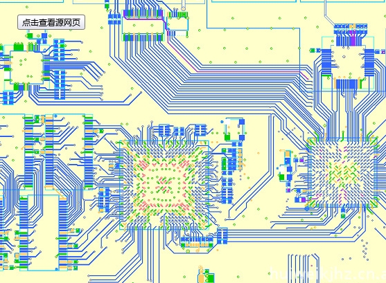
6. Layout call network table, dial in components, modify part of the size of the pad, set up wiring rules, can change the size of the label, thickness, hide the nominal value. Then place and lock the components that need special positions first. Then according to the functional module layout, (SCH can be used in the selection of the transition to PCB selection), generally do not use X, Y for component reversal, but with space rotation, or L key, (because some components can not be reversed, such as integrated block, relay, etc.). For a functional module put first center components, or components, and then put on the side of the small components, (such as integrated block is put first, and then put a direct and integrated block two pin directly connected components, put and integrated block a pin connected components, and similar components together, as far as possible more beautiful also want to consider the convenience of behind the attachment). Of course, some special components should be placed first, such as some filter capacitors and crystal oscillators should be placed close to some components first. And the components that interfere with the whole thing and stay away from it. High and low voltage modules should be separated by more than 6.4mm. Pay attention to the location of heat sink, connectors and fixers. FILL can be used in places where wiring cannot be done. Also consider heat dissipation, thermal elements.
Resistor and diode placement: divided into horizontal and vertical:
1) Flat: when the number of circuit components is not much, and the size of the circuit board is large, it is generally better to use flat; For resistance below 1/4W flat, the distance between the two pads is generally 4/10 inches, and for resistance of 1/2W flat, the distance between the two pads is generally 5/10 inches; Diode flat, 1N400X series rectifier, generally take 3/10 inch; 1N540X series rectifier tube, generally take 4 ~ 5/10 inches.
2) vertical: when the number of circuit elements is more, and the size of the circuit board is not large, the general use of vertical, vertical when the distance between the two pads generally take 1 to 2/10 inches.
7. Wiring: first set the content in the rules, VCC, GND power and other large current lines can be set wide point (0.5mm-1.5mm), generally 1mm can pass 1A current. For large voltage line spacing can be set to a large point, generally 1mm is 1000V. Set up, first cloth VCC, GND and other important lines. Note the distinction between modules. It is best to add some lines to a single panel. The holes may not be horizontal or vertical. Generally, there are no wires between solder pads of integrated blocks. The wide wires with high current can be drawn on the solder layer so that tin can be added behind. Use a 45 degree Angle for wiring.
8. Manually modify the line: modify the width of some lines, corner, tear patch or welding pad (single panel must be done), lay copper, deal with ground wire.
9. Check DRC, EMC, etc., and then you can print check, network table comparison. Component list check.
10. Add model (generally in the screen into).
11. A potentiometer is usually adjusted clockwise to increase (voltage, current, etc).
12. The high frequency (>20MHz) is generally multipoint grounded. <10MHz or <1MHz single point grounding. In between is mixed grounding.
13. As required, not all devices should be packaged in standard packages, which can be bonded or welded vertically.
14. When wiring the printed board, the position of the components on the board should be determined first, and then the ground wire and power line should be laid. When arranging high-speed signal cables, it is best to consider low-speed signal cables. The positions of the components are grouped according to the power supply voltage, digital simulation, speed, current and so on. Under safe conditions, the power cord should be as close to the ground as possible. Reducing the ring area of differential radiation also helps to reduce the interference of the circuit. When fast, medium and low speed logic circuits need to be placed on the circuit board, the high speed logic circuits should be placed near the edge of the connector, and the low speed logic and memory circuits should be placed away from the connector. This is beneficial to the reduction of common impedance coupling, radiation and interference. Grounding is the most important thing. About the time to have a backup, or some steps easy to crash, damaged files to backup.