
- 20
- Sep
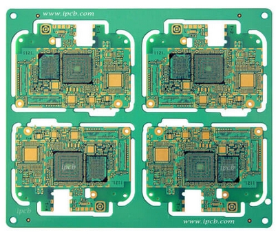
Analysis of HDI circuit board
ஆய்வு HDI PCB
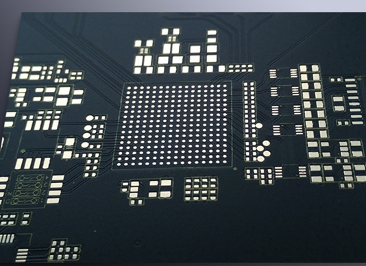
HDI stands for High Density Interconnector. It is a kind of printed circuit board that uses micro-blind and buried hole technology to produce a circuit board with High circuit distribution Density. HDI is a compact product designed for small volume users. It adopts modular parallel design, a module capacity of 1000VA (height 1U), natural cooling, can be directly placed in a 19 “rack, up to 6 modules in parallel. The product adopts full digital signal processing (DSP) technology and a number of patented technologies, with full range of load adaptability and strong short-term overload capacity, can not consider the load power factor and peak factor.
Frst stage process: 1+N+1 HDI PCB
Second order process: 2+N+2 HDI PCB
Third stage process: 3+N+3 HDI PCB
Fourth stage process: 4+N+4 HDI PCB