
- 04
- Oct
Question solving of basic knowledge of circuit board
Key production process control of high level PCB
1. Introduction to noun interpretation
Printed circuit — on the surface of an insulating material, provides a conductive pattern of electrical connections between components, including shielding elements.
Printed circuit — a circuit made of printed circuit, printed component, or a combination of the two, according to a predetermined design on the surface of insulating materials.
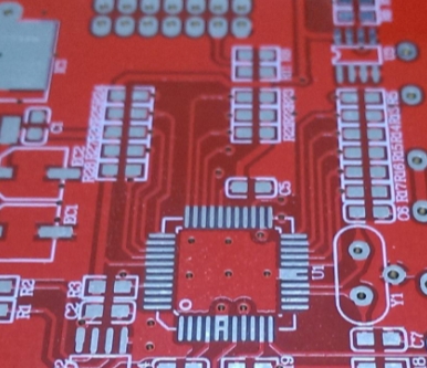
Printed circuit/circuit board — general term for insulating boards that have been finished with printed circuit or printed circuit. Mellors | | ai | | | P CB sample strips, 1, 1, ai, 1 division 1 skill the first P | 1 CB sample sheet
Low density PCB – Mass produced PCB with a wire greater than 0.3 mm (12/12mil) in width between two disks at the intersection of the 2.54 mm standard grid.
Medium density PCB – A mass-produced printed board with two wires approximately 0.2 mm (8/8mil) in width between two disks at the intersection of the 2.54 mm standard grid.
High density Printed Board — A mass-produced printed board with three wires between two disks at the intersection of a 2.54 mm standard grid width of 0.1 to 0.15 mm (4-6/4-6mil).
2. What are the types of printed circuits according to the substrate and conductive pattern used? Mellors | | ai | | | PCB sample strips, 1, 1, ai, 1 division 1 skill the first P | 1 CB sample sheet
— According to the substrate used: rigid, flexible, rigid-flexible;
— According to conductive graphics: single, double, multi-layer.
3. Describe the function of printed circuit and the characteristics of printed circuit industry.
— First of all, it provides mechanical support for PCB copy board fixing and assembly of transistors, integrated circuits, resistors, capacitors, inductors and other components.
Secondly, it realizes the wiring and electrical connection between components such as transistors, integrated circuits, resistors, capacitors and inductors, and electrical insulation to meet its electrical characteristics.
Finally, the identification characters and graphics are provided for the inspection and maintenance of components in PCB electronic assembly process, and the blocking welding graphics are provided for wave soldering.
— High technology, high investment, high risk and high profit. Mellors | | ai | | | P CB sample strips, 1, 1, ai, 1 division 1 skill the first P | 1 CB sample sheet
4. Printed circuit manufacturing process classification is mainly divided into what two methods? What are the advantages of each?
– Addition method: avoid a large number of copper etching, reduce the cost. Simplified PCB copy board production process, improve production efficiency. Flush wires and flush surfaces can be achieved. The reliability of metallized hole is improved.
– Reduction method: mature, stable and reliable process. Mellors | | ai | | | P CB sample strips, 1, 1, ai, 1 division 1 skill the first P | 1 CB sample sheet
5. What are the types of addition processes used in printed circuit manufacturing? Write out the process separately?
– Total addition method: drilling, imaging, viscosifying treatment (negative phase), electroless copper plating, removal of resist.
— Half addition method: drilling, catalytic treatment and tackification, electroless copper plating, imaging (electroplating resist), graphic electroplating copper (negative phase), removal resist, differential etching.
— Partial addition method: imaging (anti-etching), etching copper (normal phase), removing resist layer, whole plate coating electroplating resist, drilling, electroless copper plating in hole, removing electroplating resist.
6. What are the types of printed circuit in the subtraction process? Write the process flow of whole plate plating and graphic plating. Mellors | | ai | | | P CB sample strips, 1, 1, ai, 1 division 1 skill the first P | 1 CB sample sheet
— Non-perforated plated PCB, perforated plated PCB, perforated plated PCB and surface mounted PCB.
— Whole plate electroplating (masking method) : blanking, drilling, metallization of holes, thickening of whole plate electroplating, surface treatment, pasting of light masking type dry film, making normal wire graphics, etching, film removal, plug electroplating, shape processing, inspection, printing of welding resistance coating, hot air leveling, network printing of marking symbols, finished products. Mellors | | ai | | | P CB sample strips, 1, 1, ai, 1 division 1 skill the first P | 1 CB sample sheet
–PCB graphic electroplating (bare copper coating resistance film) : Double-sided copper-clad boards blanking, punching positioning hole, CNC drilling, inspection, deburring, thin thin electroless copper, electroplating copper, inspection, brush plate, sticker (or screen printing), exposure imaging (or curing), inspection retouching, electroplating copper, graphics are electroplating tin lead alloy, go to the film (or remove) was printed, inspection retouching, etching, pewter back, open circuit test, clean, resistance welding graphics, plug nickel plating / gold, plug adhesive tape, hot air leveling, cleaning, network printing symbols, shape processing, cleaning and drying, inspection, packaging, finished products.
7. Electroplating technology can be divided into what kinds of technology?
– Conventional porous plating technology, direct plating technology, conductive adhesive technology. Mellors | | ai | | | P CB sample strips, 1, 1, ai, 1 division 1 skill the first P | 1 CB sample sheet
8. What are the main features of flexible printed boards? What does its base material have?
— Flexible and foldable to reduce volume; Light weight, good wiring consistency, high reliability.
9. Describe the main features and uses of rigid – flexible PCB.
– The rigid and flexible parts are integrated, eliminating the need for connectors, reliable connection, weight reduction, assembly miniaturization. PCB copying board is mainly used in medical electronic instruments, computers and peripherals, communication equipment, aerospace equipment and national defense and military equipment. Mellors | | ai | | | P CB sample strips, 1, 1, ai, 1 division 1 skill the first P | 1 CB sample sheet
10. Describe the characteristics of conductive adhesive printed board.
– Simple processing technology, high production efficiency, low cost, less waste water.
11. What is multiple wiring PCB?
— Printed board made by layering metal wires directly on an insulating substrate.
12. What is metal – based printed board? What are its main features?
— General term for metal base printed board and metal core printed board. Mellors | | ai | | | P CB sample strips, 1, 1, ai, 1 division 1 skill the first P | 1 CB sample sheet
13. What is single-sided multilayer PCB? What are its main features?
Manufacture of multilayer circuit boards on a single PCB. PCB board characteristics: not only can restrain the internal electromagnetic wave to the outside radiation, but also can prevent the interference of external electromagnetic wave to it, does not need the hole metallization, low cost, light weight, can be thin.
14. Brief introduction to the definition and manufacture of multilayer printed circuit?
— A high density multi-layer wiring printed board is made by alternating insulating layer and conductive layer in the way of stacking layer on the inner layer of the completed multi-layer board, and blind holes are freely used to conduct between layers.