
- 18
- Sep
PCB (printed circuit board) Introduction
Printed Circuie Board (PCB) is short for Printed circuit Board. Usually in insulation material, according to the predetermined design, made of printed circuit, printed components or a combination of both conductive graphics called printed circuit. The conductive graph of the electrical connection between components provided on the insulating substrate is called printed circuit. In this way, the printed circuit or printed line of the finished board is called printed circuit board, also known as printed board or printed circuit board.

PCB is indispensable for almost all electronic equipment we can see, from electronic watches, calculators and general computers to computers, communication electronic equipment and military weapon systems. As long as there are no electronic components such as integrated circuits, PCB is used for the electrical interconnection between them. It provides mechanical support for fixed assembly of various electronic components such as integrated circuits, realizes wiring and electrical connection or electrical insulation between various electronic components such as integrated circuits, and provides required electrical characteristics, such as characteristic impedance, etc. At the same time to provide automatic solder blocking graph; Provide identification characters and graphics for component installation, inspection and maintenance.
How are PCBS made? When we open the thumb drive of a general-purpose computer, we can see a soft film (flexible insulating substrate) printed with silver-white (silver paste) conductive graphics and potential graphics. Because of the universal screen printing method to get this graph, so we call this printed circuit board flexible silver paste printed circuit board. Different from the motherboards, graphics cards, network cards, modems, sound cards and printed circuit boards on home appliances we see in Computer City. The base material used is made of paper base (usually used for single side) or glass cloth base (often used for double-sided and multi-layer), pre-impregnated phenolic or epoxy resin, one or both sides of the surface glued with copper book and then laminated curing. This kind of circuit board covers copper book board, we call it rigid board. Then we make a printed circuit board, we call it a rigid printed circuit board. A printed circuit board with printed circuit graphics on one side is called a single-sided printed circuit board, and a printed circuit board with printed circuit graphics on both sides is interconnected on both sides through the metallization of holes, and we call it a double-panel. If using a double lining, two one-way for outer layer or two double lining, two blocks of single outer layer of the printed circuit board, through the positioning system and alternate insulation adhesive materials and conductive graphics interconnection according to design requirement of printed circuit board becomes four, six layer printed circuit board, also known as multilayer printed circuit board. There are now more than 100 layers of practical printed circuit boards.
The production process of PCB is relatively complex, which involves a wide range of processes, from simple mechanical processing to complex mechanical processing, including common chemical reactions, photochemistry, electrochemistry, thermochemistry and other processes, computer-aided design (CAM) and other knowledge. And in the process of production process problems and will always meet new problems and some problems in didn’t find out the reason disappears, because its production process is a kind of continuous line form, any link wrong would caused production across the board or the consequences of a large number of scrap, printed circuit board if there is no recycling scrap, Process engineers can be stressful, so many engineers leave the industry to work in sales and technical services for PCB equipment or materials companies.
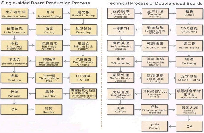
PCB-ni daha yaxşı başa düşmək üçün ümumiyyətlə bir tərəfli, iki tərəfli çaplı elektron kartın və adi çox qatlı lövhənin istehsal prosesini başa düşmək lazımdır.
Single-sided rigid printed board: – single copper clad – blanking to scrub, dry), drilling or punching – > screen printing lines etched pattern or using dry film resistance to curing check fix plate, copper etching and dry to resist printing material, to scrub, dry, screen printing resistance welding graphics (commonly used green oil), UV curing to character marking graphics screen printing, UV curing, preheating, punching, and the shape – electric open and short circuit test – scrubbing, drying → pre-coating welding anti-oxidant (dry) or tin-spraying hot air leveling → inspection packaging → finished products factory.
Double-sided rigid printed board: – double-sided copper-clad boards – blanking – laminated – nc drill guide hole – inspection, deburring scrub – chemical plating (guide hole metallization) – thin copper plating (full board) – inspection scrub – > screen printing negative circuit graphics, cure (dry film/wet film, exposure and development) – inspection and repairing the plate – line graphics plating and electroplating tin (corrosion resistance of nickel/gold) – > to print material (coating) – etching copper – (annealing tin ) to scrub clean, commonly used graphics screen printing resistance welding heat curing green oil (photosensitive dry film or wet film, exposure, development and heat curing, often heat curing photosensitive green oil) and dry cleaning, to screen printing mark character graphics, curing, (tin or organic shielded welding film) to form processing, cleaning, drying to electrical on-off testing, packaging and finished products.
Through hole metallization method of manufacturing a multilayer process flow to the inner layer copper clad double-sided cutting, scrub to drill positioning hole, stick to the dry coating or coating to resist to exposure, development and etching and film – the inner coarsening and oxidation – inner check – (outer line production of single-sided copper clad laminates, B – bonding sheet, plate bonding sheet inspection, drill positioning hole) to laminate, several control drilling – > Hole and check before treatment and chemical copper plating – full board and thin copper plating coating inspection – stick to resistance to dry film plating or coating to plating agent to coat bottom exposure, development and fix the plate – line graphics electroplating – or nickel/gold plating and electroplating tin lead alloy to film and the etching – check – screen printing resistance welding graphics or light induced resistance welding graphics – printed character graphics – (hot air leveling or organic shielded welding film) and numerical control Washing shape → cleaning, drying → electrical connection detection → finished product inspection → packing factory.
It can be seen from the process flow chart that the multilayer process is developed from the two-face metallization process. In addition to the two-sided process, it has several unique contents: metallized hole inner interconnect, drilling and epoxy decontamination, positioning system, lamination, and special materials.
Our common computer board card is basically epoxy glass cloth double-sided printed circuit board, which has one side is inserted components and the other side is the component foot welding surface, can see that the solder joints are very regular, the component foot discrete welding surface of these solder joints we call it the pad. Why don’t the other copper wires have tin on them? Because in addition to the solder plate and other parts of the need for soldering, the rest of the surface has a layer of wave resistance welding film. Its surface solder film is mostly green, and a few use yellow, black, blue, etc., so the solder oil is often called green oil in THE PCB industry. Its function is to prevent wave welding bridge phenomenon, improve welding quality and save solder and so on. It is also a permanent protective layer of printed board, can play the role of moisture, corrosion, mildew and mechanical abrasion. From the outside, the surface is smooth and bright green blocking film, which is photosensitive to the film plate and heat curing green oil. Not only the appearance is better, it is important that the pad accuracy is high, so as to improve the reliability of the solder joint.
As we can see from the computer board, components are installed in three ways. A plug-in installation process for transmission in which an electronic component is inserted into a through-hole on a printed circuit board. It is easy to see that the double-sided printed circuit board through holes are as follows: one is a simple component insert hole; The second is the component insertion and double-sided interconnection through hole; Three is a simple double-sided through hole; Four is the base plate installation and positioning hole. The other two mounting methods are surface mounting and chip mounting directly. In fact, chip direct mounting technology can be considered as a branch of surface mounting technology, it is the chip directly glued to the printed board, and then connected to the printed board by wire welding method or belt loading method, flip method, beam lead method and other packaging technology. The welding surface is on the component surface.
Səth montaj texnologiyası aşağıdakı üstünlüklərə malikdir:
(1) Because of the large through hole or buried hole interconnection technology is largely eliminated by the printed board, the wiring density on the printed board is improved, the area of the printed board is reduced (generally one third of the plug-in installation), and the number of design layers and cost of the printed board can also be reduced.
(2) Reduced weight, improved seismic performance, the use of colloidal solder and new welding technology, improve product quality and reliability.
(3) Due to the increase of wiring density and lead length, the parasitic capacitance and parasitic inductance are reduced, which is more conducive to improving the electrical parameters of the printed board.
(4) It is easier to realize automation than plug-in installation, improve installation speed and labor productivity, and reduce assembly cost accordingly.
As can be seen from the above surface safety technology, the improvement of circuit board technology is improved with the improvement of chip packaging technology and surface mounting technology. The computer board that we see now card its surface stick installs rate to rise ceaselessly. In fact, this kind of circuit board reuse transmission screen printing line graphics is unable to meet the technical requirements. Therefore, the ordinary high precision circuit board, its line graphics and welding graphics are basically sensitive circuit and sensitive green oil production process.
With the development trend of high density circuit board, the production requirements of circuit board are becoming higher and higher. More and more new technologies are applied to the production of circuit board, such as laser technology, photosensitive resin and so on. The above is just some superficial introduction of the surface, there are many things in the production of circuit board due to space constraints, such as blind hole, winding board, teflon board, photolithography and so on. If you want to study in depth, you need to work hard.