
- 19
- May
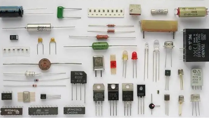
On line pin sequence of electronic components
For the vast majority of electronic components, they have polarity, or the pins can not be soldered wrong. For example, once the electrolytic capacitor is welded reversely, it will explode when energized. Generally speaking, when using automatic feeding machinery to assemble circuit board components, there will be no problem of misplacing components. However, due to the limitations of manufacturers and the characteristics of components, not all components can be automatically pasted or inserted. Common manual placement is required for various surface mounted transformers, connectors, to encapsulated integrated circuits, etc. These devices may still have the problem of assembly error. Generally, the repair is carried out manually, and this link is also prone to the problem of reverse welding. Therefore, it is necessary to explain the positioning method of components and the corresponding relationship between component pads and silk screen printing on the circuit board.
1. Capacitance
For the electrolytic capacitor installed in the aluminum through hole shown in the figure below, the positive and negative poles are generally represented by the long and short feet and the mark on the body. The long leg is positive and the short leg is negative. Generally, there are white or other stripes parallel to the pin on the shell of the negative side.
The electrolytic capacitor on the circuit board is generally marked with polarity as shown in the figure.
One method is to mark a “+” sign directly on the positive side. The advantage of this method is that it is convenient to check the polarity after welding. The disadvantage is that it occupies a large area of the circuit board. The second method is to fill the area where the negative electrode is located with silk screen. This polarity representation occupies a small area of the circuit board, but it is inconvenient to check the polarity after welding. It is common in occasions with high density of circuit board devices such as computer motherboard.
Tantalum capacitors installed through holes are generally marked with “+” on the body on the positive side, and some varieties are further distinguished by long and short feet.
The marking method on the circuit board of this capacitor can refer to aluminum electrolytic capacitor.
For surface mounted aluminum electrolytic capacitors. The side coated with ink is the negative pole, and the base on the positive pole side is generally chamfered.
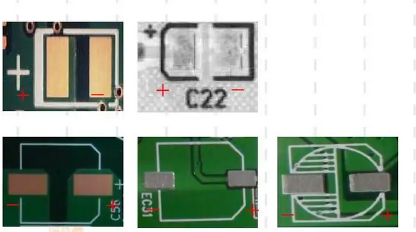 On the Printed Circuit Board, it is generally shown in the figure above
That is to use silk screen “+” on the circuit board to represent the positive pole, and draw the outline of the device at the same time. In this way, the chamfered side can also be used to identify the positive electrode.
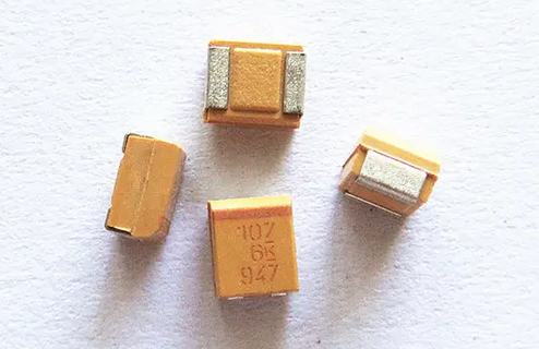
Surface bonded tantalum capacitor
2. Diode
For light-emitting diodes, the long and short pins are generally used to represent the positive and negative poles. The long pin is positive and the short pin is negative. Sometimes the manufacturer will cut off a little on one side of the LED, which can also be used to represent the negative electrode.
Silk screen “+” is generally used on the circuit board to indicate the positive electrode.
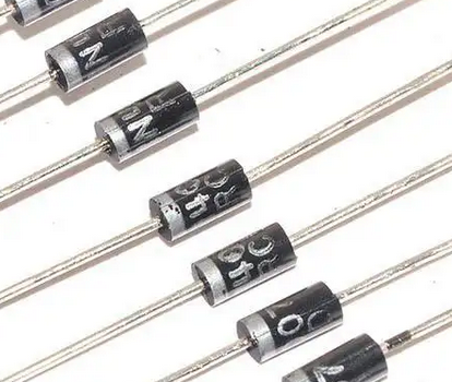
For ordinary diodes
In the figure above, the left side is the negative pole and the right side is the positive pole, that is, silk screen printing or stained glass is used to represent the positive and negative polarity. The following two methods are generally used to represent the positive and negative polarity on the circuit board.
The polarity of the diode is indicated by the silk screen on the circuit board. This is more vivid. The other is to draw the schematic symbols of diodes directly on the silk screen printed circuit board.
The polarity representation of surface mounted LED is very confusing. Sometimes there are various representations between different package types in a manufacturer. However, it is common to paint color spots or color strips on the cathode side of light-emitting diodes. There are also corners cut on the cathode side.
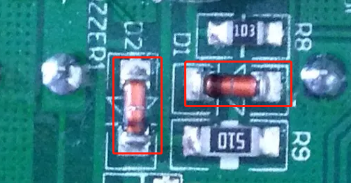
Ordinary surface mount diodes also use silk screen printing or stained glass on the body to represent the negative electrode
Integrated circuit
For dip and so packaged integrated circuits with pins distributed on both sides, the upper semicircular notch is generally used to indicate that this direction is above the chip, and the first pin on the upper left is the first pin of the chip. It is also indicated by a horizontal line on the top with silk screen printing or laser.
In addition, there are also silk screen dots directly on the body next to the first pin of the chip or pressing a pit directly during injection molding.
Some integrated circuits are also represented by cutting a beveled edge on the body of the starting edge of the first pin.
The symbols of this kind of integrated circuit on the circuit board are generally marked with a gap on the top.
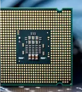
For QFP, PLCC and BGA in tetragonal package.
QFP packaged integrated circuits generally use concave dots, silk screen dots, or silk screen printing according to the model to judge the direction on the body corresponding to the first pin. Some use the method of cutting off an angle to represent the first foot. At this time, the counterclockwise direction is the first foot. It should be noted that sometimes there are three pits on a chip, so a corner without pits corresponds to the lower right of the chip.
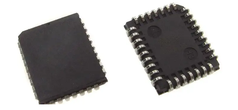
Because the body of PLCC package is relatively large, it is generally represented by pits directly at the beginning of the first pin. Some also cut corners at the top left of the chip.
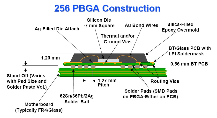
BGA packaged object
BGA packaging not only uses the gold-plated copper foil in the lower left corner to represent the first pin, but also uses the way of missing corners, pits and silk screen dots to represent the direction of the first pin.
The graphics on the corresponding circuit board are as follows
 The first leg is treated with silk screen dots and missing corners.
4. other devices
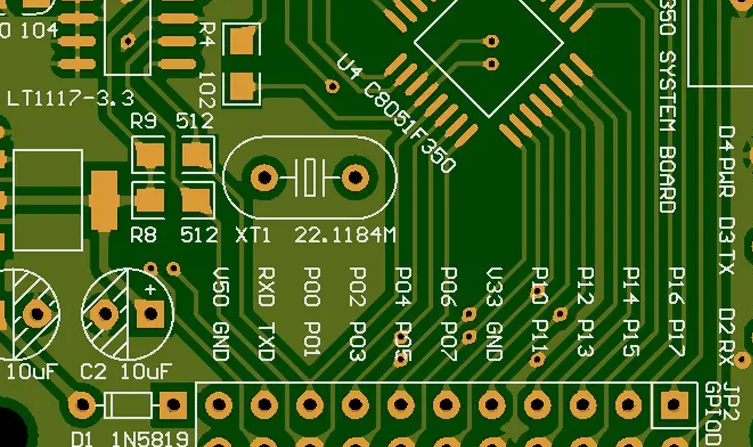
In the real object, the connector generally controls the direction by positioning the notch. There are also those who write 1 near the first foot or use triangle to represent the first foot. Generally speaking, other devices avoid wrong insertion by drawing silk screen consistent with the real object on the printed circuit board.
For the resistance removal of through-hole installation, it is generally expressed by wrapping the common end with silk screen on the circuit board. Or write 1 near the first foot.
In order to standardize the requirements of pad, silk screen printing and resistance welding of components on circuit board, IPC organization has issued two related standards: ipc-7351 and ipc-sm-840. However, in actual use, the device direction marking symbols made by the device direction representation method defined by IPC are often blocked by the device body after welding, which is not suitable for inspection. The graphic design of component pad should be adjusted according to the actual situation.
In short, in real objects, generally discrete devices use the methods of long and short feet, silk screen printing or coloring to represent the polarity. For integrated circuits, concave points, silk screen printing, notches, missing corners, missing edges or direct indication are often used for the first pin marking. When making pad graphics, generally draw according to the device shape as much as possible, and reflect the information related to positioning on the device shape in the form of silk screen as much as possible, so as to avoid errors in manual assembly and welding.