
- 19
- May
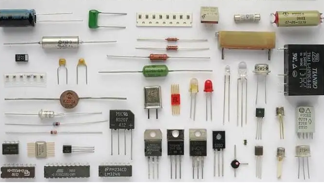
Sekwencja pinów online komponentów elektronicznych
W przypadku zdecydowanej większości elementów elektronicznych mają one biegunowość lub nie da się źle wlutować pinów. Na przykład, gdy kondensator elektrolityczny zostanie zespawany odwrotnie, wybuchnie po włączeniu zasilania. Ogólnie rzecz biorąc, przy użyciu automatycznych maszyn podających do montażu elementów płytki drukowanej, nie będzie problemu z nieprawidłowym umieszczeniem elementów. Jednak ze względu na ograniczenia producentów i charakterystykę komponentów nie wszystkie komponenty można automatycznie wkleić lub wstawić. Wspólne ręczne umieszczanie jest wymagane dla różnych transformatorów montowanych powierzchniowo, złączy, do hermetyzowanych układów scalonych itp. Urządzenia te mogą nadal mieć problem z błędem montażu. Generalnie naprawa jest wykonywana ręcznie, a to ogniwo również jest podatne na problem ze spawaniem wstecznym. Dlatego konieczne jest wyjaśnienie metody pozycjonowania komponentów i odpowiedniego związku między padami komponentów a sitodrukiem na płytce drukowanej.
1. Pojemność
For the electrolytic capacitor installed in the aluminum through hole shown in the figure below, the positive and negative poles are generally represented by the long and short feet and the mark on the body. The long leg is positive and the short leg is negative. Generally, there are white or other stripes parallel to the pin on the shell of the negative side.
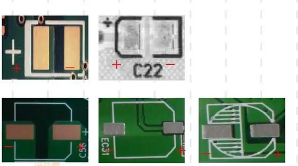
Kondensator elektrolityczny na płytce drukowanej jest ogólnie oznaczony biegunowością, jak pokazano na rysunku.
Jedną z metod jest zaznaczenie znaku „+” bezpośrednio po stronie dodatniej. Zaletą tej metody jest wygodna kontrola polaryzacji po spawaniu. Wadą jest to, że zajmuje dużą powierzchnię płytki drukowanej. Druga metoda polega na wypełnieniu sitodrukiem obszaru, w którym znajduje się elektroda ujemna. Ta reprezentacja biegunowości zajmuje niewielką powierzchnię płytki drukowanej, ale niewygodne jest sprawdzanie biegunowości po spawaniu. Jest to powszechne w przypadku dużej gęstości urządzeń z obwodami drukowanymi, takich jak płyta główna komputera.
Kondensatory tantalowe instalowane przez otwory są generalnie oznaczone „+” na korpusie po stronie dodatniej, a niektóre odmiany wyróżniają się długimi i krótkimi stopkami.
Metoda znakowania na płytce drukowanej tego kondensatora może odnosić się do aluminiowego kondensatora elektrolitycznego.
Do aluminiowych kondensatorów elektrolitycznych do montażu powierzchniowego. Strona pokryta tuszem jest biegunem ujemnym, a podstawa po stronie bieguna dodatniego jest zwykle sfazowana.
 Na Płytka drukowana, jest to ogólnie pokazane na powyższym rysunku
That is to use silk screen “+” on the circuit board to represent the positive pole, and draw the outline of the device at the same time. In this way, the chamfered side can also be used to identify the positive electrode.
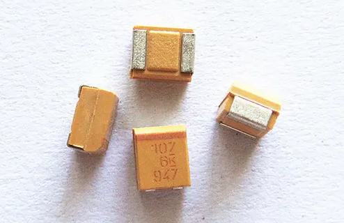
Kondensator tantalowy z wiązaniem powierzchniowym
2. Dioda
W przypadku diod elektroluminescencyjnych długie i krótkie styki są zwykle używane do reprezentowania biegunów dodatnich i ujemnych. Długa szpilka jest dodatnia, a krótka szpilka ujemna. Czasami producent odcina trochę po jednej stronie diody LED, która może być również używana do reprezentowania elektrody ujemnej.
Sitodruk „+” jest zwykle używany na płytce drukowanej do wskazania elektrody dodatniej.
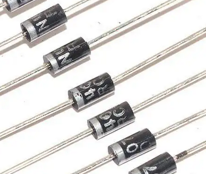
For ordinary diodes
In the figure above, the left side is the negative pole and the right side is the positive pole, that is, silk screen printing or stained glass is used to represent the positive and negative polarity. The following two methods are generally used to represent the positive and negative polarity on the circuit board.
Polaryzacja diody jest wskazywana przez sitodruk na płytce drukowanej. To jest bardziej żywe. Drugim jest narysowanie schematycznych symboli diod bezpośrednio na sitodruku Płytka drukowana.
The polarity representation of surface mounted LED is very confusing. Sometimes there are various representations between different package types in a manufacturer. However, it is common to paint color spots or color strips on the cathode side of light-emitting diodes. There are also corners cut on the cathode side.
Polaryzacja diody jest wskazywana przez sitodruk na płytce drukowanej. To jest bardziej żywe. Drugim jest narysowanie schematycznych symboli diod bezpośrednio na płytce drukowanej z sitodrukiem.
The polarity representation of surface mounted LED is very confusing. Sometimes there are various representations between different package types in a manufacturer. However, it is common to paint color spots or color strips on the cathode side of light-emitting diodes. There are also corners cut on the cathode side.
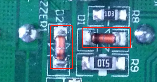
Ordinary surface mount diodes also use silk screen printing or stained glass on the body to represent the negative electrode
Układ scalony
W przypadku dipowych i tak upakowanych układów scalonych z pinami rozmieszczonymi po obu stronach, górne półkoliste wcięcie jest zwykle używane do wskazania, że kierunek ten znajduje się nad chipem, a pierwszy pin w lewym górnym rogu jest pierwszym pinem chipa. Wskazuje na to również pozioma linia na górze z sitodrukiem lub laserem.
In addition, there are also silk screen dots directly on the body next to the first pin of the chip or pressing a pit directly during injection molding.
Niektóre układy scalone są również reprezentowane przez wycięcie ściętej krawędzi na korpusie krawędzi początkowej pierwszego pinu.
The symbols of this kind of integrated circuit on the circuit board are generally marked with a gap on the top.
For QFP, PLCC and BGA in tetragonal package.
Umieszczone w obudowie układy scalone QFP zazwyczaj używają wklęsłych kropek, kropek sitodruku lub sitodruku zgodnie z modelem, aby ocenić kierunek na korpusie odpowiadający pierwszej szpilce. Niektórzy używają metody odcinania kąta, aby przedstawić pierwszą stopę. W tej chwili kierunek przeciwny do ruchu wskazówek zegara to pierwsza stopa. Należy zauważyć, że czasami na żetonie znajdują się trzy dołki, więc róg bez dołków odpowiada dolnemu prawu żetonu.
Ponieważ korpus pakietu PLCC jest stosunkowo duży, jest on zazwyczaj reprezentowany przez wgłębienia bezpośrednio na początku pierwszego pinu. Niektórzy również ścinają rogi w lewym górnym rogu żetonu.
Obiekt w pakiecie BGA
BGA packaging not only uses the gold-plated copper foil in the lower left corner to represent the first pin, but also uses the way of missing corners, pits and silk screen dots to represent the direction of the first pin.
The graphics on the corresponding circuit board are as follows
 Pierwsza noga jest pokryta kropkami z sitodruku i brakującymi rogami.
4. inne urządzenia
In the real object, the connector generally controls the direction by positioning the notch. There are also those who write 1 near the first foot or use triangle to represent the first foot. Generally speaking, other devices avoid wrong insertion by drawing silk screen consistent with the real object on the Płytka drukowana.
For the resistance removal of through-hole installation, it is generally expressed by wrapping the common end with silk screen on the circuit board. Or write 1 near the first foot.
In order to standardize the requirements of pad, silk screen printing and resistance welding of components on circuit board, IPC organization has issued two related standards: ipc-7351 and ipc-sm-840. However, in actual use, the device direction marking symbols made by the device direction representation method defined by IPC are often blocked by the device body after welding, which is not suitable for inspection. The graphic design of component pad should be adjusted according to the actual situation.
In short, in real objects, generally discrete devices use the methods of long and short feet, silk screen printing or coloring to represent the polarity. For integrated circuits, concave points, silk screen printing, notches, missing corners, missing edges or direct indication are often used for the first pin marking. When making pad graphics, generally draw according to the device shape as much as possible, and reflect the information related to positioning on the device shape in the form of silk screen as much as possible, so as to avoid errors in manual assembly and welding.