
- 05
- Oct
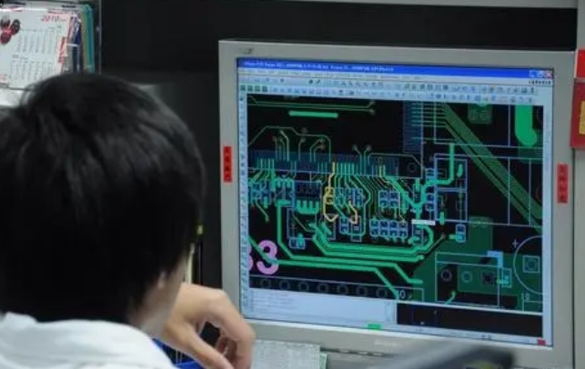
Six summaries of PCB production design
Six summaries of PCB production design
1. Layout
First, consider the size of PCB. When the size of PCB circuit board is too large, the printed line is long, the impedance increases, the anti noise ability decreases and the cost increases; If it is too small, the heat dissipation is poor, and the adjacent lines are easy to be disturbed. After determining the size of PCB, determine the position of special components. Finally, all components of the circuit are arranged according to the functional units of the circuit.
The following principles shall be observed when determining the position of special elements:
(1) Shorten the wiring between high-frequency components as much as possible, and try to reduce their distribution parameters and mutual electromagnetic interference. Components susceptible to interference shall not be too close to each other, and input and output components shall be as far away as possible.
(2) There may be high potential difference between some components or wires, so the distance between them should be increased to avoid accidental short circuit caused by discharge. Components with high voltage shall be arranged in places not easy to touch during commissioning.
(3) The position occupied by the positioning hole of the printed plate and the fixed support shall be reserved.
According to the functional unit of the circuit, the layout of all components of the circuit shall comply with the following principles:
(1) Arrange the position of each functional circuit unit according to the circuit flow, make the layout convenient for signal flow, and keep the signal in the same direction as far as possible.
(2) Take the core components of each functional circuit as the center and layout around it. The components shall be evenly, neatly and compactly arranged on the PCB. The leads and connections between components shall be reduced and shortened as far as possible.
(3) For the circuit working at high frequency, the distribution parameters between components should be considered. For general circuits, components shall be arranged in parallel as far as possible. In this way, it is not only beautiful, but also easy to assemble and weld, and easy to mass produce.
(4) Components located at the edge of the circuit board are generally not less than 2mm away from the edge of the circuit board. The best shape of the circuit board is rectangle. The aspect ratio is 3:2 to 4:3. When the surface size of the circuit board is greater than 200x150mm, the mechanical strength of the circuit board shall be considered.
2. Wiring
The principles of wiring are as follows:
(1) The conductors used at the input and output terminals shall avoid adjacent parallel as far as possible. It is better to add ground wire between lines to avoid feedback coupling.
(2) The minimum width of the printed conductor is mainly determined by the adhesion strength between the conductor and the insulating base plate and the current flowing through them.
(3) The bend of printed wire is generally circular arc, and the right angle or included angle will affect the electrical performance in high-frequency circuit. In addition, try to avoid using large-area copper foil, otherwise, copper foil expansion and falling off are easy to occur when heated for a long time. When a large area of copper foil must be used, it is best to use grid shape, which is conducive to eliminating the volatile gas generated by the heating of the adhesive between the copper foil and the substrate.
3. Pad
The pad center hole (in-line device) is slightly larger than the device lead diameter. If the pad is too large, it is easy to form false soldering. The outer diameter D of the pad is generally not less than (D + 1.2) mm, where D is the lead hole diameter. For high-density digital circuits, the minimum diameter of pad can be (D + 1.0) mm.
Anti interference measures for PCB and circuit:
The anti-interference design of printed circuit board is closely related to the specific circuit. Here, only a few common measures of PCB anti-interference design are described.
1. Power cord design
According to the current of the printed circuit board, try to increase the width of the power line and reduce the loop resistance. At the same time, make the direction of power line and ground wire consistent with the direction of data transmission, which helps to enhance the anti noise ability.
2. Lot design
The principles of ground wire design are:
(1) Digital and analog are separated. If there are both logic circuits and linear circuits on the circuit board, they shall be separated as far as possible. Single point parallel grounding shall be adopted for the grounding of low-frequency circuit as far as possible. If it is difficult to connect the actual wiring, it can be partially connected in series and then connected in parallel. Multi point series grounding shall be adopted for high-frequency circuit, the ground wire shall be short and rented, and grid like large-area ground foil shall be used around high-frequency components as far as possible.
(2) The grounding wire shall be as thick as possible. If the grounding wire is made of sewn wire, the grounding potential changes with the change of current, so that the anti noise performance is reduced. Therefore, the grounding wire should be thickened so that it can pass three times the allowable current on the printed board. If possible, the grounding wire shall be more than 2 ~ 3mm.
(3) The grounding wire forms a closed loop. For printed boards only composed of digital circuits, the grounding circuit is arranged in a cluster loop, which can improve the anti noise ability.
4. Decoupling capacitor configuration
One of the conventional methods of PCB design is to configure appropriate decoupling capacitors at each key part of the PCB. The general configuration principle of decoupling capacitor is:
(1) The power input terminal is connected with 10 ~ 100uF electrolytic capacitor. If possible, it is better to connect more than 100uF.
(2) In principle, each integrated circuit chip shall be equipped with a 0.01uF ~ 0.1uF ceramic chip capacitor. In case of insufficient gap in the printed board, a 1 ~ 10PF capacitor can be arranged every 4 ~ 8 chips.
(3) For devices with weak noise resistance and large power change during shutdown, such as RAM and ROM storage devices, decoupling capacitors shall be directly connected between the power line and ground wire of the chip.
5. Through hole design
In high-speed PCB design, seemingly simple vias often bring great negative effects to the circuit design. In order to reduce the adverse effects caused by the parasitic effects of vias, we can try our best in the design
(1) Considering the cost and signal quality, a reasonable via size is selected. For example, for 6-10 layer memory module PCB design, it is better to select 10 / 20MIL (drilling / pad) vias. For some high-density small-size boards, you can also try to use 8 / 18mil vias. Under the current technical conditions, it is difficult to use smaller through holes (when the depth of the hole exceeds 6 times the drilling diameter, it is impossible to ensure that the hole wall can be uniformly plated with copper); For vias of power or ground, larger size can be considered to reduce impedance
(2) The signal routing on PCB board shall not change layers as far as possible, that is, unnecessary vias shall not be used as far as possible
(3) The pins of the power supply and the ground should be perforated nearby. The shorter the lead between the via and the pin, the better
(4) Place some grounded vias near the vias of signal layer change to provide the nearest circuit for the signal. You can even place a large number of redundant grounding vias on the PCB
6. Some experience in reducing noise and electromagnetic interference
(1) If you can use low-speed chips, you don’t need high-speed ones. High-speed chips are used in key places
(2) A series of resistors can be used to reduce the jump rate of the upper and lower edges of the control circuit.
(3) Try to provide some form of damping for relays, etc., such as RC setting current damping
(4) Use the lowest frequency clock that meets the system requirements.
(5) The clock shall be as close as possible to the device using the clock. The shell of the quartz crystal oscillator shall be grounded. The clock area shall be surrounded by ground wire. The clock line shall be as short as possible. There shall be no wiring under the quartz crystal and under the noise sensitive device. Clock, bus and chip selection signals shall be far away from I / O line and connector. The interference of clock line perpendicular to I / O line is less than that parallel to I / O line
(6) The input end of the unused gate circuit shall not be suspended, the positive input end of the unused operational amplifier shall be grounded, and the negative input end shall be connected to the output end