
- 05
- Oct
Common problems and countermeasures in FPC and PCB production process
Common problems and countermeasures in FPC og PCB produktions proces
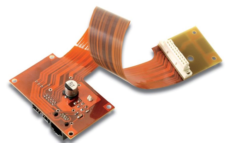
With the transformation of surface welding to lead-free type, PCB circuit board needs to bear ultra-high welding temperature, and the demand for thermal shock resistance of external surface solder resist layer is higher and higher. The demand for terminal surface treatment, peeling strength of solder resist layer (ink, masking film) and adhesion with base copper is higher and higher. We need a better pre-treatment technology to ensure. By improving our technology, we can improve the yield of goods and achieve profit growth. High quality pre-treatment potion can undoubtedly help us at a low cost.
This article mainly introduces the questions and Countermeasures often encountered in the production process of PCB and FPB soft circuit board: first, the line section presents side erosion and concave appearance when etching the line after dry film or wet film treatment, resulting in lack of line width or uneven line. The reason is nothing more than improper selection of dry and wet film data, improper exposure parameters and poor function of exposure machine. Development, etching section nozzle conditioning, unreasonable conditioning of related parameters, improper concentration and scale of liquid medicine, improper transmission speed and other series can cause questions. However, we often find that there is no abnormality by checking the above parameters and related equipment functions, but there are still questions such as over corrosion and concave corrosion of the circuit board when making the board. What is the reason after all?
2、 When doing PCB pattern electroplating and surface treatment of PCB and FPC terminals, such as gold deposition, electric gold, electric tin, chemical tin and other technical treatment, we often find that the boards produced show the appearance of infiltration plating at the edge of dry and wet film or solder resist layer, or most of the boards or some of the local boards, No matter what kind of situation, it will bring unnecessary cancellation or defects, unnecessary trouble for post-processing, and even cancellation at the end, which is heartbreaking! The reason is that we usually think of the dry and wet film parameters, and the data function is in doubt; There are questions about solder resist, such as ink for hard board, masking film for soft board, or questions in printing, pressing, curing and other sections. Indeed, each of these places can cause this doubt. Then we are also confused that there is no doubt or doubt in the above step section, but it will still show the appearance of infiltration plating. After all, what’s the reason for not finding out?
3、 PCB boards will be tested with tin before shipment. Of course, customers will use tin welded components. There is a doubt that the ink can be significantly peeled or that the peeling strength of the masking film of the soft plate is lack or uneven, Customers, especially those who do fine SMT mounting, can’t bear such questions. Once the solder resist layer presents the appearance of light peeling during welding, it will make it impossible to accurately mount the original, resulting in the loss of many components and work delays by customers. The circuit board factory will face huge losses such as deduction, material supplement, and even loss of customers. So what aspects do we usually start with when we encounter such questions? We usually analyze whether it is solder resist (ink, masking film) data; Is there any doubt during silk screen printing, lamination and curing; Is there any doubt about electroplating potion? wait… Therefore, we usually order engineers to find out the reason and improve from these sections. We also wonder if it’s the climate? It’s relatively wet recently, and the board absorbs moisture? (PCB substrate and barrier are easy to absorb moisture) through some hard work, they can harvest some effects. It is doubtful that they will be treated externally for the time being.