
- 06
- Oct
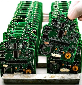
How to prevent six phenomena of tin connection on circuit board after wave soldering.
How to prevent six phenomena of tin connection on circuit board after wave soldering.
1. Due to the phenomenon of tin connection caused by too long component pin during wave soldering of circuit board, attention shall be paid to the extension length of component pin is generally 1.5-2mm, which will not occur if it does not exceed this height.
2. Because the PCB process design is more and more complex and the lead pin spacing is more and more dense, the phenomenon of tin connection after wave soldering occurs. Changing the pad design is the solution. For example, reducing the pad size, increasing the length of the pad exiting the wave side, increasing the flux activity / reducing the lead extension length are also the solutions.
3. After wave soldering, the molten tin infiltrates the surface of the circuit board to form the tin connection between the component pins. The main reason for this phenomenon is that the inner diameter of the empty pad is too large, or the outer diameter of the pin of the component is too small.
4. The wave crest formed by dense foot components in two areas is connected with tin after welding.
5. Wave soldering with tin due to excessive pad size.
6. Tin connection of component pins after wave soldering due to poor solderability of component pins.
Method for preventing tin connection of circuit board after wave soldering.
1. Design according to PCB design specification. The long axis of the two end chips shall be perpendicular to the welding direction, and the long axis of SOT and SOP shall be parallel to the welding direction. Widen the pad of the last pin of SOP (design a solder pad);
2. The pins of inserted components shall be formed according to the hole spacing and assembly requirements of the printed board. If the short insertion welding process is adopted, the component pins on the welding surface shall be exposed to the surface of the printed board by 0.8 ~ 3mm, and the component body shall be upright during insertion;
3. Set the preheating temperature according to the PCB size, whether there are multilayer boards, the number of components, the number of mounted components, etc;
4. The tin wave temperature is 250 ± 5 ℃, and the welding time is 3 ~ 5S. When the temperature is slightly lower, the speed of the conveyor belt should be slower;
5. Replace the flux.