
- 04
- Oct
Key production process control for high level circuit board
The high-level PCB is generally defined as 10 layers — 20 layers or more of the high multi-layer circuit board. It is more difficult to process than the traditional multi-layer circuit board, and its quality and reliability requirements are high. It is mainly used in communication equipment, high-end servers, medical electronics, aviation, industrial control, military and other fields. In recent years, the demand of high-rise board market in applied communication, base station, aviation, military and other fields is still strong, and with the rapid development of China’s telecom equipment market, the prospect of high-rise board market is promising.
At present, the large-scale production of high-level PCB manufacturers in China mainly come from foreign-funded enterprises or a small number of domestic enterprises. The production of high-level circuit board not only requires higher technology and equipment investment, but also requires the accumulation of experience of technical personnel and production personnel. At the same time, the import of high-level board customer certification procedures are strict and cumbersome, so the high-level circuit board enters the enterprise with a higher threshold, and the industrialization production cycle is longer. The average number of PCB layers has become an important technical index to measure the technical level and product structure of PCB enterprises. This paper briefly describes the main processing difficulties encountered in the production of high-level circuit board, and introduces the key control points of the key production process of high-level circuit board for your reference.
One, the main production difficulties
Compared with the characteristics of conventional circuit board products, the high-level circuit board has the characteristics of thicker board parts, more layers, more dense lines and holes, larger unit size, thinner medium layer, etc., and the inner space, inter-layer alignment, impedance control and reliability requirements are more stringent.
1.1 Difficulty of interlayer alignment
Due to the large number of high-rise board layers, the client design end has more and more strict requirements on the alignment of PCB layers. Usually, the alignment tolerance between layers is controlled to be ±75μm. Considering the large size of high-rise board element design, the ambient temperature and humidity of graphic transfer workshop, and the dislocation superposition caused by the inconsistency of expansion and contraction of different core board layers, the positioning mode between layers and other factors, It makes it more difficult to control the alignment between layers of the high-rise board.
1.2 Difficulties in making inner circuit
The high-rise board adopts special materials such as high TG, high speed, high frequency, thick copper, thin medium layer, etc., which puts forward high requirements on the inner circuit fabrication and graphic size control, such as the integrity of impedance signal transmission, which increases the difficulty of inner circuit fabrication. Line width line distance is small, open short circuit increase, micro short increase, low pass rate; There are more signal layers in the dense line, and the probability of AOI missing detection in the inner layer increases. The thickness of the inner core plate is thin, easy to fold resulting in poor exposure, easy to roll plate when etching; Most of the high-rise boards are system boards, and the unit size is large, so the cost of finished product scrap is relatively high.
1.3 Difficulty of pressing production
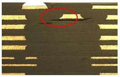
Multiple inner core plates and semi-cured plates are superimposed, and defects such as slide plate, lamination, resin cavity and bubble residue are easily produced during pressing production. In the design of laminated structure, it is necessary to fully consider the material’s heat resistance, voltage resistance, the amount of glue and the thickness of the medium, and set a reasonable high – rise plate pressing program. Because of the large number of layers, the expansion and shrinkage control and the size coefficient compensation can not keep the consistency; The thin insulation layer between layers easily leads to the failure of reliability test between layers. Figure 1 is the defect diagram of burst plate delamination after thermal stress test.
1.4 Difficult points in drilling
Special copper plates with high TG, high speed, high frequency and thick thickness are used to increase the difficulty of drilling roughness, burr and decontaminate. The number of layers, total copper thickness and plate thickness, easy to break the knife drilling; CAF failure caused by dense BGA and narrow hole wall spacing; The thickness of the plate can easily lead to the problem of skew drilling.
Ii. Control of key production processes
2.1 Material Selection
With high performance processing for electronic components, more functional in the direction of development, at the same time with high frequency, high speed development of signal transmission, so the electronic circuit material dielectric constant and dielectric loss is low, and low CTE, low water absorption and high performance copper clad material better, to satisfy the requirement of the top plate processing and reliability. Commonly used plate suppliers mainly include A series, B series, C series and D series. See Table 1 for the comparison of the main characteristics of these four inner substrate. For top thick half solidification of copper circuit board selects high resin content, interlayer half of solidification layer of resin flow is enough to graphics fill, dielectric layer is too thick easy to appear the finished plate super thick, whereas slants thin, dielectric layer is easy to result in layered medium, high pressure test failure such as quality problem, so the choice of dielectric material is very important.
2.2 Laminated structure design
In the design of the laminated structure, the main factors to be considered are the heat resistance of the material, the voltage resistance, the amount of glue and the thickness of the medium layer, etc. The following main principles should be followed.
(1) The semi-cured piece and the core plate manufacturer must be consistent. In order to ensure PCB reliability, all layers of semi-cured tablets should avoid using A single 1080 or 106 semi-cured tablets (except for special requirements of customers). When there is no requirement of medium thickness, the thickness of medium between layers must be ≥0.09mm according to IPC-A-600g.
(2) When the customer requires high TG plate, the core plate and semi-cured plate should use the corresponding high TG material.
(3) Inner substrate 3OZ or above, select high resin content of semi-cured tablets, such as 1080R/C65%, 1080HR/C 68%, 106R/C 73%, 106HR/C76%; However, the structural design of 106 semi-cured sheets with high adhesive should be avoided as much as possible to prevent the overlapping of multiple 106 semi-cured sheets. Because the glass fiber yarn is too thin, the collapse of glass fiber yarn in the large substrate area will affect the dimensional stability and the lamination of the explosion plate.
(4) If the customer does not have special requirements, the thickness tolerance of interlayer medium is generally controlled by +/-10%. For impedance plate, the thickness tolerance of medium is controlled by IPC-4101 C/M tolerance. If the impedance influencing factor is related to the thickness of the substrate, the plate tolerance must also be controlled by IPC-4101 C/M tolerance.
2.3 Interlayer alignment control
The accuracy of inner core panel size compensation and production size control need to be based on the data and historical data collected in production in a certain period of time to accurately compensate the graphic size of each layer of the upper panel to ensure the consistency of the expansion and contraction of each layer of the core panel. Select high-precision and highly reliable interlamination positioning before pressing, such as four-slot positioning (Pin LAM), hot melt and rivet combination. The key to ensure the quality of pressing is to set up appropriate pressing process and daily maintenance of the press, control the pressing glue and cooling effect, and reduce the problem of dislocation between layers. Interlayer alignment control needs to be considered comprehensively from the inner layer compensation value, pressing positioning mode, pressing process parameters, material properties and other factors.
2.4 Inner line process
Because the analytical capacity of traditional exposure machine is about 50μm, for the production of high-level board, laser direct imager (LDI) can be introduced to improve the graphic analytical capacity, the analytical capacity of about 20μm. The alignment accuracy of traditional exposure machine is ±25μm, and the interlayer alignment accuracy is greater than 50μm. The positioning accuracy of the graph can be improved to about 15μm and the interlayer positioning accuracy can be controlled within 30μm by using high-precision positioning exposure machine, which reduces the positioning deviation of traditional equipment and improves the interlayer positioning accuracy of the high-rise board.
In order to improve the line etching ability, it is necessary to give proper compensation to the width of the line and the pad (or welding ring) in the engineering design, but also need to do more detailed design consideration to the compensation amount of special graphics, such as loop circuit, independent circuit and so on. Confirm whether the design compensation for inner line width, line distance, isolation ring size, independent line, hole-to-line distance is reasonable, or change the engineering design. The design of impedance and inductive reactance requires attention to whether the design compensation of independent line and impedance line is enough. The parameters are well controlled when etching, and the first piece can be mass produced after being confirmed as qualified. In order to reduce etching side erosion, it is necessary to control the composition of etch solution in the best range. The traditional etching line equipment has insufficient etching ability, so the equipment can be technically modified or imported into high-precision etching line equipment to improve the etching uniformity, reduce the etching burr, etching impurity and other problems.
2.5 Pressing process
At present, the interlayer positioning methods before pressing mainly include: four-slot positioning (Pin LAM), hot melt, rivet, hot melt and rivet combination. Different product structures adopt different positioning methods. For high level plates, four-slot positioning (Pin LAM), or fusion + riveting, OPE punches out the positioning holes with accuracy controlled to ±25μm. During the batch production, it is necessary to check whether each plate is fused into the unit to prevent subsequent stratification. The pressing equipment adopts high-performance supporting press to meet the interlayer alignment accuracy and reliability of the high-rise plate.
According to the top plate laminated structure and the materials used, the appropriate pressing procedures, set the best heating rate and curve, on regular multilayer PCB pressing procedures, appropriate to reduce the pressing sheet metal heating rate, extended high temperature curing time, make the resin flow, curing, at the same time avoid the skateboard in the process of pressing, interlayer displacement problem. Material TG value is not the same board, can not be the same grate board; Ordinary parameters of the board can not be mixed with special parameters of the board; To ensure the reasonableness of expansion and contraction coefficient, the performance of different plates and semi-cured sheets is different, and the corresponding semi-cured sheet parameters should be used for pressing, and the special materials that have never been used need to verify the process parameters.
2.6 Drilling process
Due to the superposition of each layer, the plate and copper layer are super thick, which causes serious wear on the drill bit and is easy to break the drill tool. The number of holes, falling speed and rotating speed should be appropriately lowered. Accurately measure the expansion and contraction of the plate, providing accurate coefficient; The number of layers ≥14, hole diameter ≤0.2mm or hole to line distance ≤0.175mm, the use of hole accuracy ≤0.025mm drill production; Step drilling is used for diameter φ4.0mm or above, step drilling is used for thickness to diameter ratio 12:1, and positive and negative drilling is used for production. Control the drilling front and hole diameter. Try to use a new drill knife or grind 1 drill knife to drill the upper board. The hole diameter should be controlled within 25um. In order to solve the burr problem of drilling hole of thick copper plate in high level, it is proved by batch test that using high density pad, stacking plate number is one and drilling bit grinding time is controlled within 3 times can effectively improve burr of drilling hole
For high frequency, high speed and mass data transmission of high board, back drilling technology is an effective way to improve signal integrity. The back drill mainly controls the length of residual stub, the consistency of hole location between two drilling holes and the copper wire in the hole. Not all driller equipment has back drilling function, it is necessary to carry out technical upgrade of driller equipment (with back drilling function), or purchase a driller with back drilling function. The back drilling techniques used in relevant industry literature and mature mass production mainly include: traditional depth control back drilling method, back drilling with signal feedback layer in the inner layer, calculation of depth back drilling according to the ratio of plate thickness, which will not be repeated here.
Three, reliability test
The high-level board is generally the system board, thicker than the conventional multilayer board, heavier, larger unit size, the corresponding heat capacity is also larger, in the welding, the need for more heat, the welding high temperature time is long. It takes 50 to 90 seconds at 217℃ (melting point of tin-silver-copper solder), and the cooling speed of the high-rise plate is relatively slow, so the test time of the reflow welding is extended. In combination with ipC-6012C, IPC-TM-650 standards and industry requirements, the main reliability test of the high-rise plate is described in Table 2.
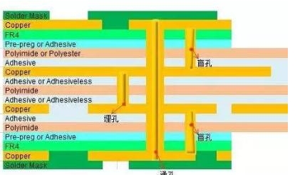
Table2